Substrate-guided optical device

a technology of optical devices and substrates, applied in the field of substrate-guided optical devices, can solve the problems of inconvenient installation, inconvenient use, and inconvenient use, and achieve the effects of convenient design and fabrication, large emb values, and easy incorporation

Active Publication Date: 2010-03-18
LUMUS LTD
View PDF9 Cites 52 Cited by
  • Summary
  • Abstract
  • Description
  • Claims
  • Application Information

AI Technical Summary

Benefits of technology

[0006]The present invention facilitates the design and fabrication of very compact light-guide optical elements (LOE) for, amongst other applications, head-mounted displays. The invention allows relatively wide FOVs together with relatively large EMB values. The resulting optical system offers a large, high-quality image, which also accommodates large movements of the eye. The optical system offered by the present invention is particularly advantageous because it is substantially more compact than state-of-the-art implementations, and yet it can be readily incorporated even into optical systems having specialized configurations.

Problems solved by technology

Nevertheless, state-of-the-art HUDs suffer several significant drawbacks.
As a result, the combiner-projector HUD system is necessarily bulky and large, and requires a considerable installation space, which makes it inconvenient for installation and at times even unsafe to use.
The large optical aperture of conventional HUDs also poses a significant optical design challenge, rendering the HUDs with either compromised performance, or leading to high cost wherever high-performance is required.
The limiting factor remains the quality of the display within the device of the end-user.
The mobility requirement restricts the physical size of the displays, and the result is a direct-display with a poor image viewing quality.

Method used


Image

  • Substrate-guided optical device
  • Substrate-guided optical device
  • Substrate-guided optical device

Examples


Embodiment Construction

[0032]The present invention relates to substrate-guided optical devices and particularly to devices which include a plurality of reflecting surfaces carried by a common light-transmissive substrate or to a LOE.

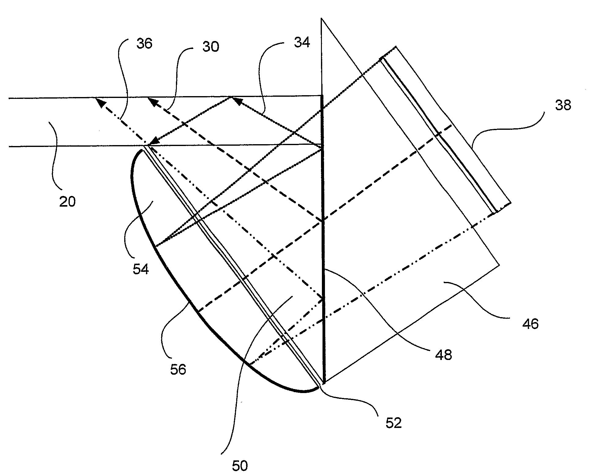
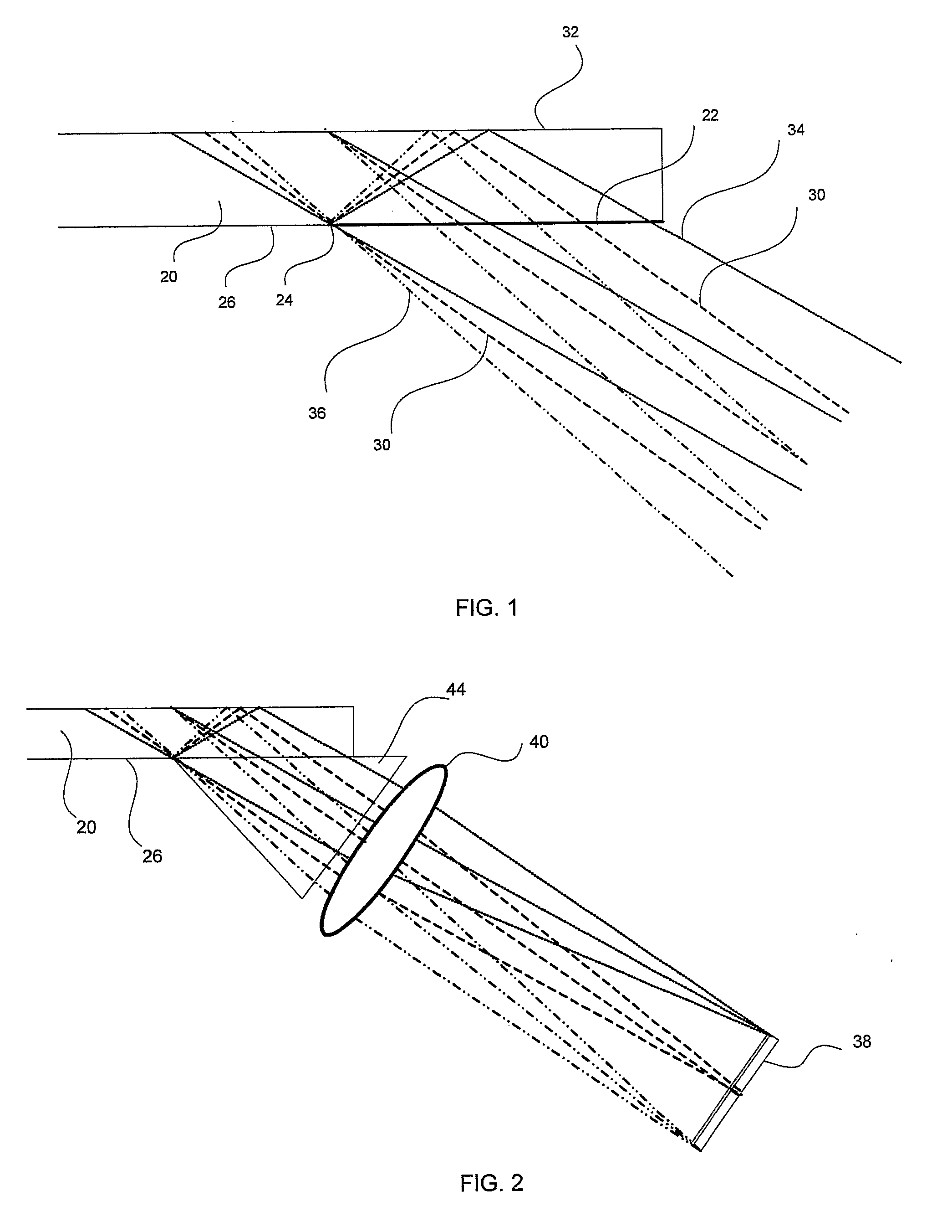
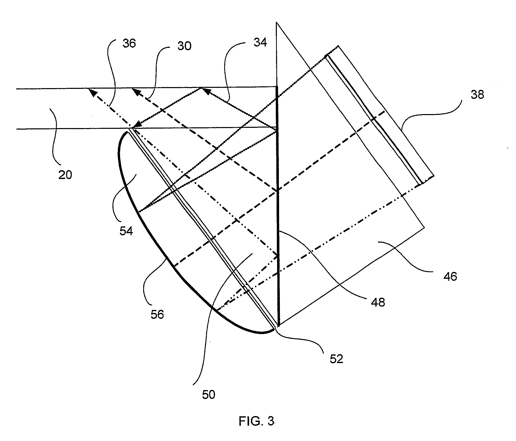
[0033]According to the object of the present invention to find a coupling-in mechanism different to the coupling-in mechanism of the prior art, replacing the typically used input mirror, there is illustrated in FIG. 1 a span of rays that have to be coupled into a LOE, e.g., a substrate 20, with a minimal required input aperture 21. In order to avoid an image with gaps or stripes, the points on the boundary line 24, between the edge of input aperture 21 and the lower surface 26 of the substrate 20, should be illuminated for each one of the input light waves by two different rays that enter the substrate from two different locations: one ray 30 that illuminates the boundary line 24 directly, and another ray 31, which is first reflected by the upper surface 32 before illuminating...


PUM


Abstract

There is provided an optical device, including a light-transmitting substrate (20) having an input aperture and first and second major surfaces (26, 32) parallel to each other and edges, one partially reflecting surface located in the substrate which is non-parallel to the major surfaces of the substrate and an optical arrangement having an output aperture for coupling light into the substrate by total internal reflection. The optical arrangement for coupling light is located outside of the substrate, the output aperture is optically attached to the input aperture of the substrate and the part of the substrate located next to the substrate input aperture, is substantially transparent.

Description

FIELD OF THE INVENTION[0001]The present invention relates to substrate-guided optical devices, and particularly to devices which include a plurality of reflecting surfaces carried by a common light-transmissive substrate, also referred to as a light-guide element.[0002]The invention can be implemented to advantage in a large number of imaging applications, such as head-mounted and head-up displays, cellular phones, compact displays, 3-D displays, compact beam expanders, as well as non-imaging applications like flat-panel indicators, compact illuminators and scanners.BACKGROUND OF THE INVENTION[0003]One of the important applications for compact optical elements is in head-mounted displays where an optical module serves both as an imaging lens and a combiner, in which a two-dimensional display is imaged to infinity and reflected into the eye of an observer. The display can be obtained directly from either a spatial light modulator (SLM) such as a cathode ray tube (CRT), a liquid cryst...

Claims


Application Information

Patent Timeline
Patent Type & Authority Applications(United States)
IPC IPC(8): G02B27/14G02B27/28G02B27/01
CPCG02B5/30G02B6/00G02B2027/0125G02B27/0172G02B27/286G02B27/0081G02B5/04G02B27/0101G02B27/14
Inventor HADAD, MALIAMITAI, YAAKOV
Owner LUMUS LTD
Why Eureka
Try Eureka