

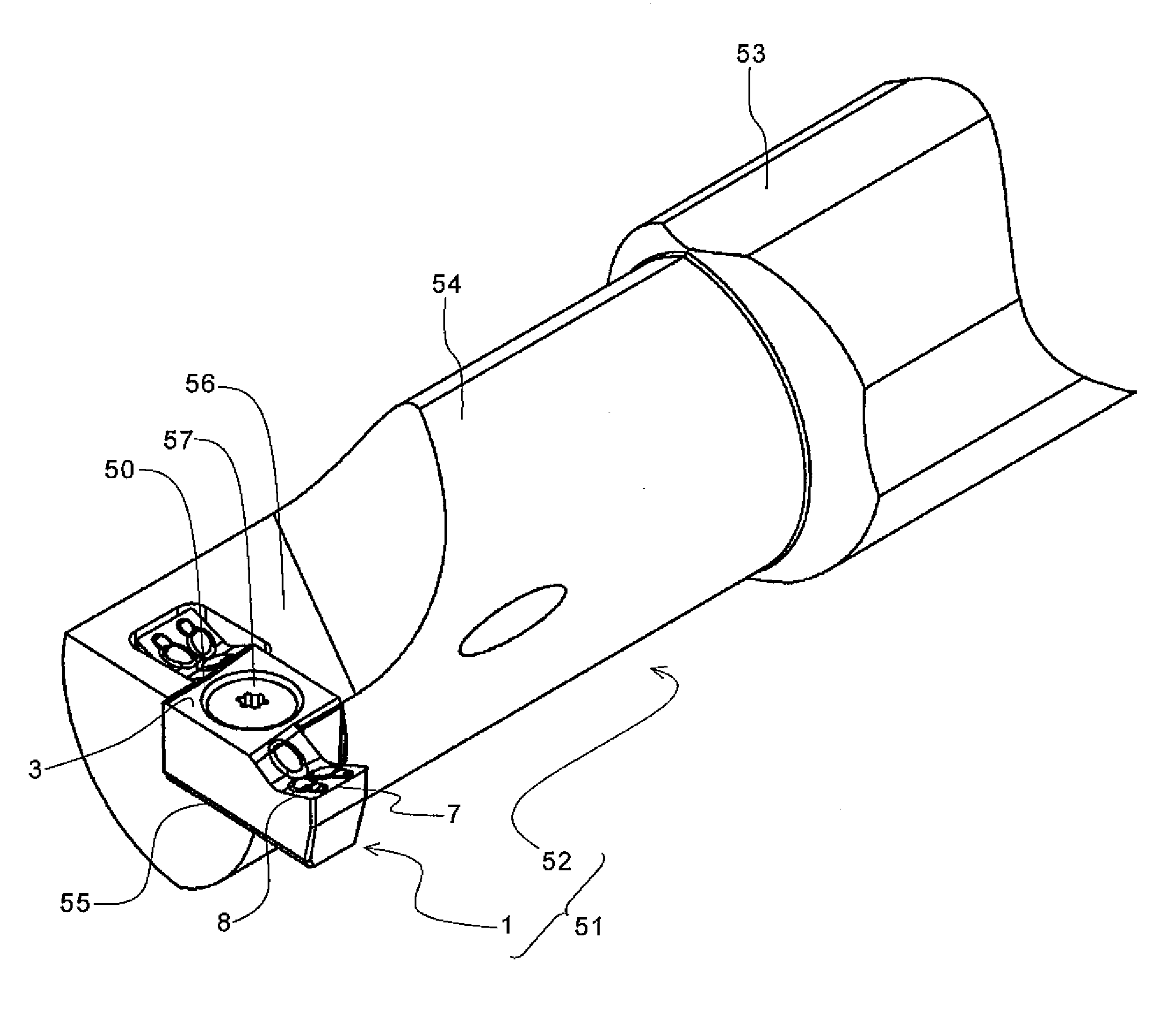
Cutting Insert
a cutting insert and insert technology, applied in the field of cutting inserts, can solve the problems of cutting inserts b>100/b> being damaged, machined surfaces might be damaged, and cutting inserts might be damaged, and achieve the effect of excellent chip discharge properties
- Summary
- Abstract
- Description
- Claims
- Application Information
AI Technical Summary
Benefits of technology
Problems solved by technology
Method used
Image

Examples
example 1
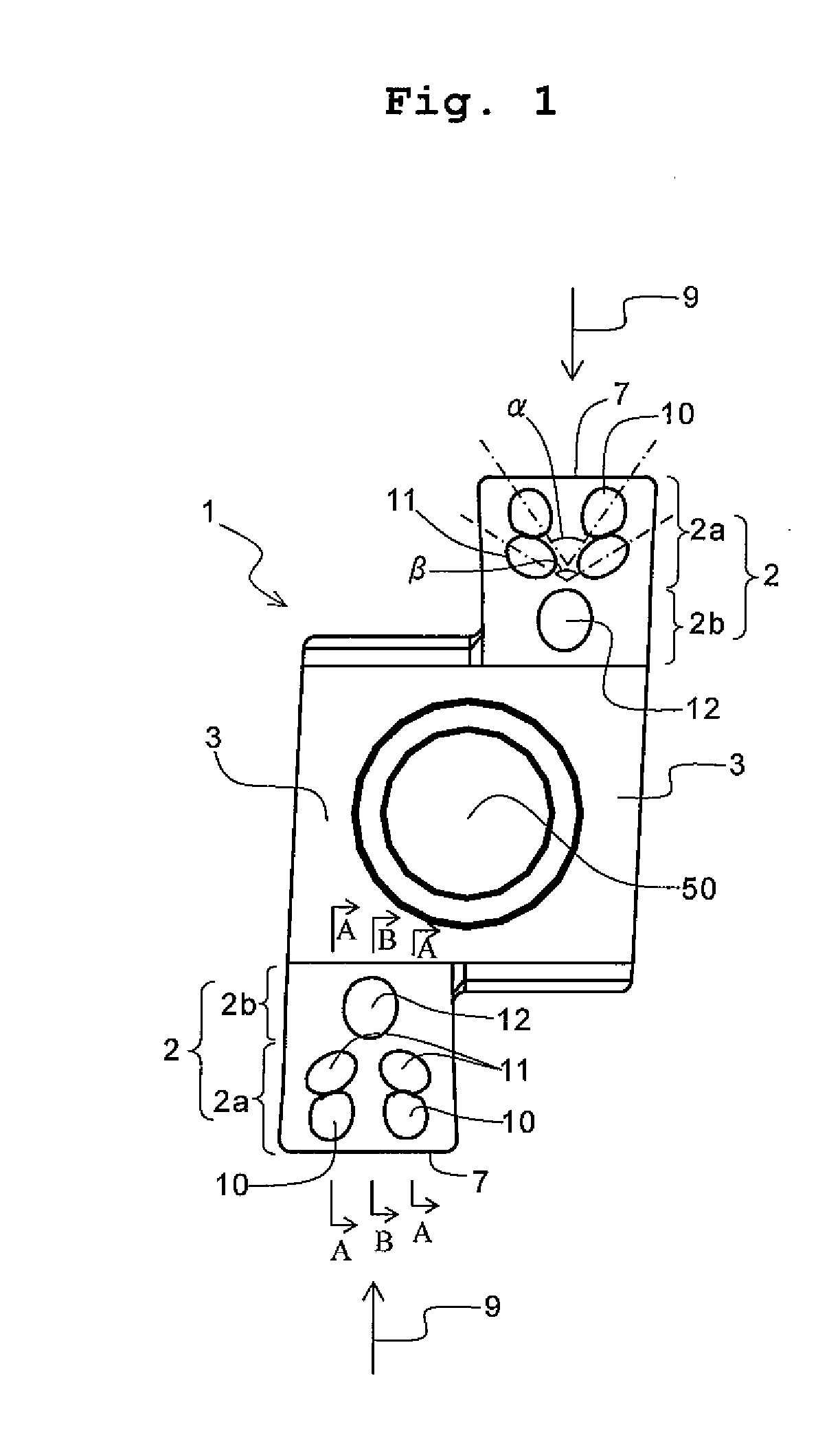
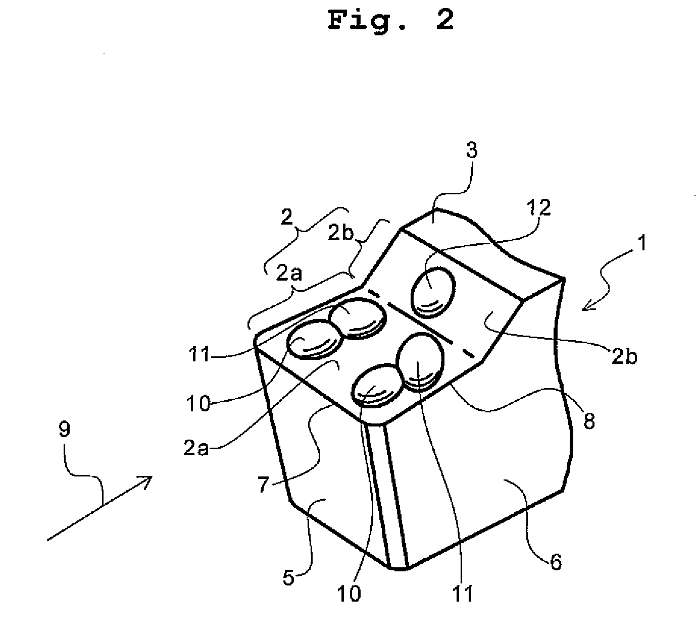
[0101]The insert 1 having the configuration shown in FIG. 1 as described above was manufactured. Specifically, the insert main body of the insert 1 was composed of coated cemented carbide having a hard thin film coated on the surface of a sintered cemented carbide body. The dimensions of the insert 1 are as follows. As the projection height, the thickness direction dimension from the boundary line between the projection and the rake face to the top portion of the projection (the dimension in the direction substantially perpendicular to the mounting surface of the holder) was measured in the section passing through the top portion of the projection and substantially parallel to the front cutting edge 7 and substantially perpendicular to the rake face. As the major axis length and minor axis length, the maximum dimensions perpendicular to an imaginary symmetrical axis in the plane view were measured, respectively. As the length of the flat surface 4, the dimension along a flat surface...
example 2
[0131]The insert 1 of Example 1 was used to evaluate the influence of the first projection 10 on the section of the chip 60. Specifically, as shown in FIG. 19, the evaluation was made by visually observing a plurality of sections of the generated chip 60. As a result, it was found that the section at a specific point had a characteristic sectional shape, and the sections at other points had a similar shape.
[0132]In FIG. 19, the point corresponding to the point having the similar sectional shape is plotted as Ia, and the specific point is plotted as Ib. The results thereof are shown in FIGS. 20(a) and (b). FIG. 20(a) shows the section of the chip 60 at the Ia in FIG. 19, and FIG. 20(b) shows the section of the chip 60 at the Ib in FIG. 19. The Ib having the characteristic sectional shape was 1 mm apart from the tip end of the chip 60.
[0133]As apparent from FIGS. 20(a) and (b), it can be seen that the section of the chip 60 is transformed from the section shown in FIG. 20(a) to the se...
PUM
| Property | Measurement | Unit |
|---|---|---|
| distance | aaaaa | aaaaa |
| distances | aaaaa | aaaaa |
| length | aaaaa | aaaaa |
Abstract
Description
Claims
Application Information