

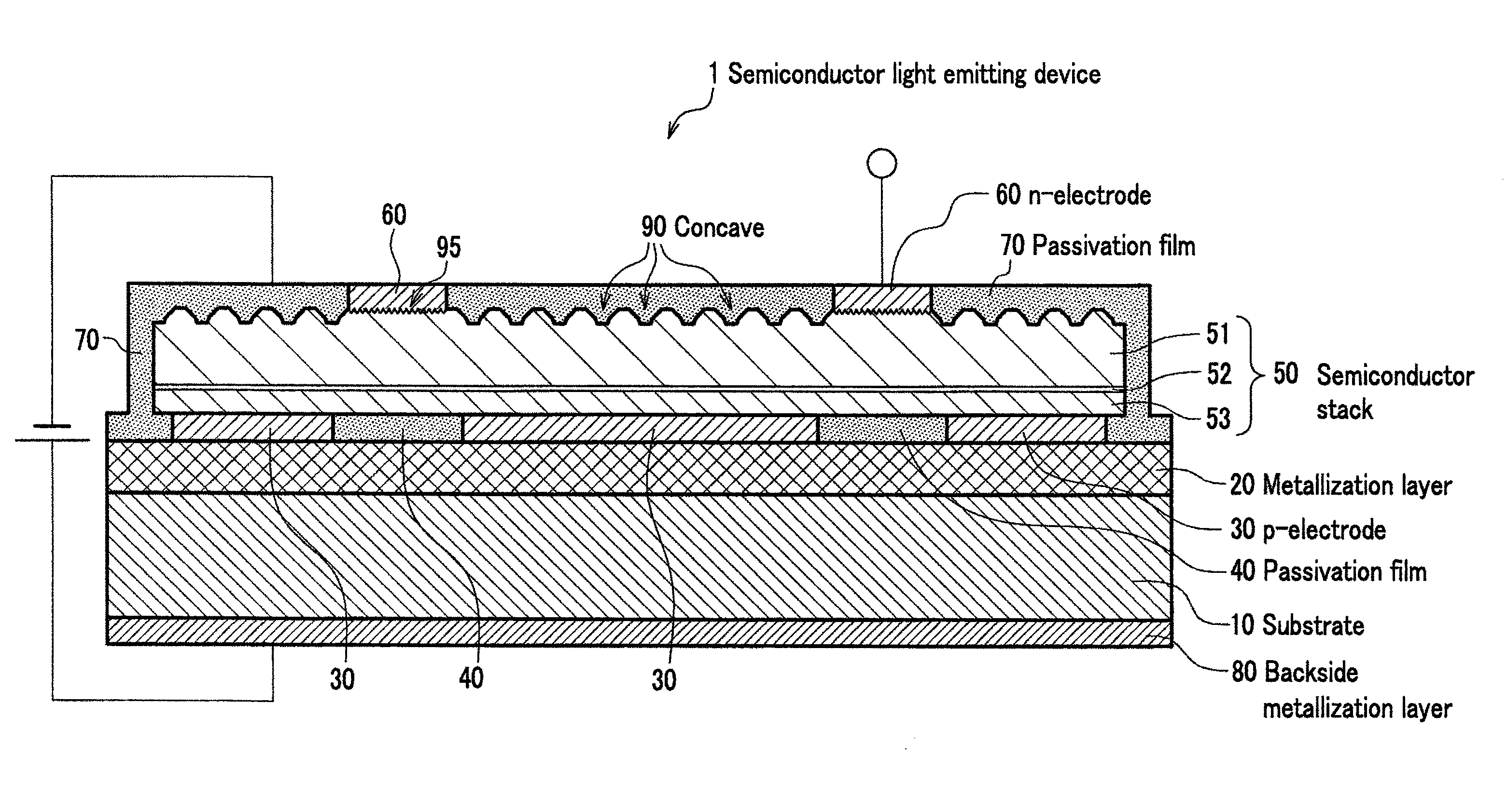
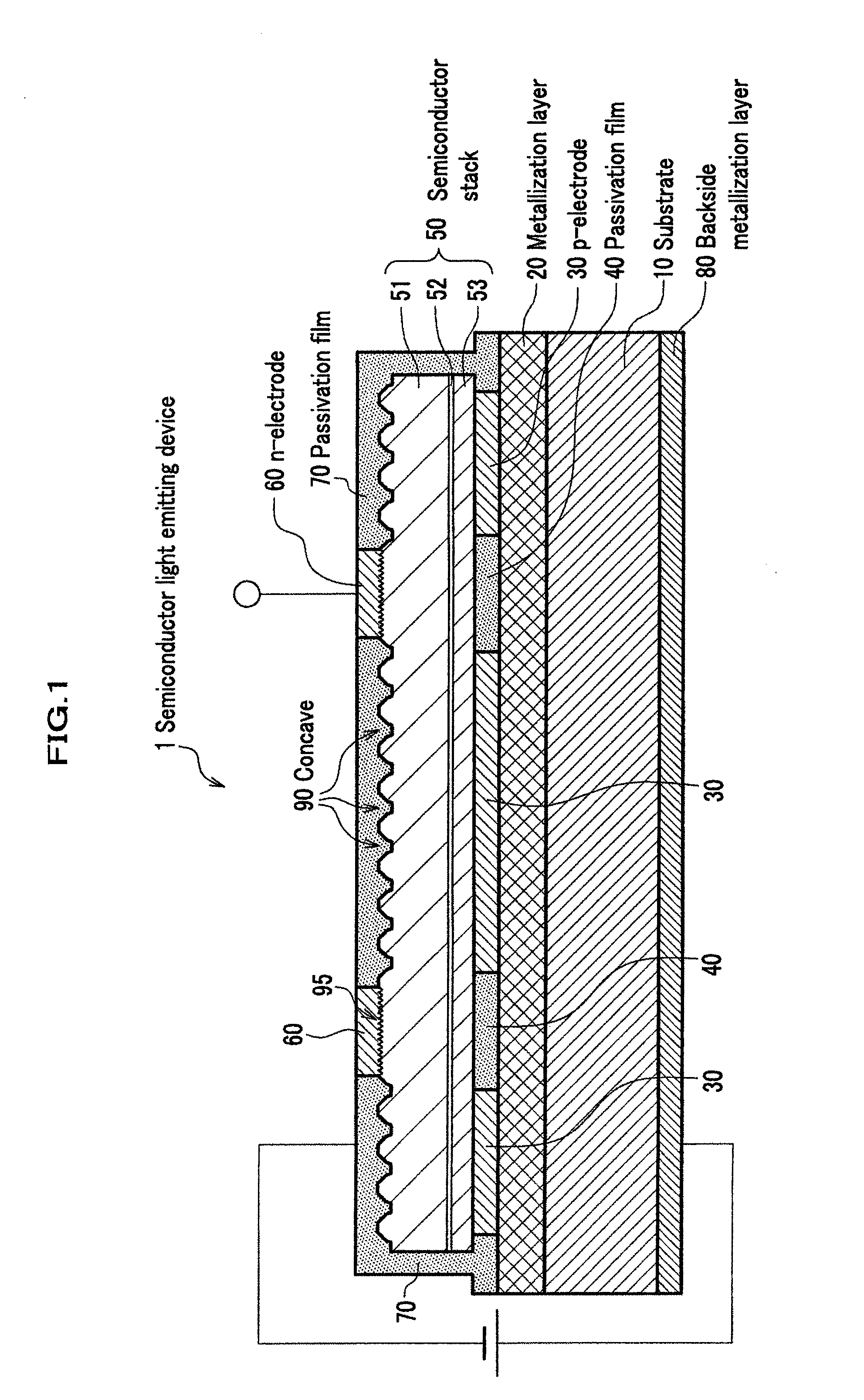
Semiconductor light emitting device
a technology of light-emitting devices and semiconductors, which is applied in the direction of semiconductor devices, basic electric elements, electrical appliances, etc., can solve the problems of poor light distribution, poor light distribution, and low extraction efficiency of light emitted outside from the convex in the right upward direction, and achieves easy and uniform diffusion, good light distribution, and easy and uniform diffusion.
- Summary
- Abstract
- Description
- Claims
- Application Information
AI Technical Summary
Benefits of technology
Problems solved by technology
Method used
Image

Examples
first modified example
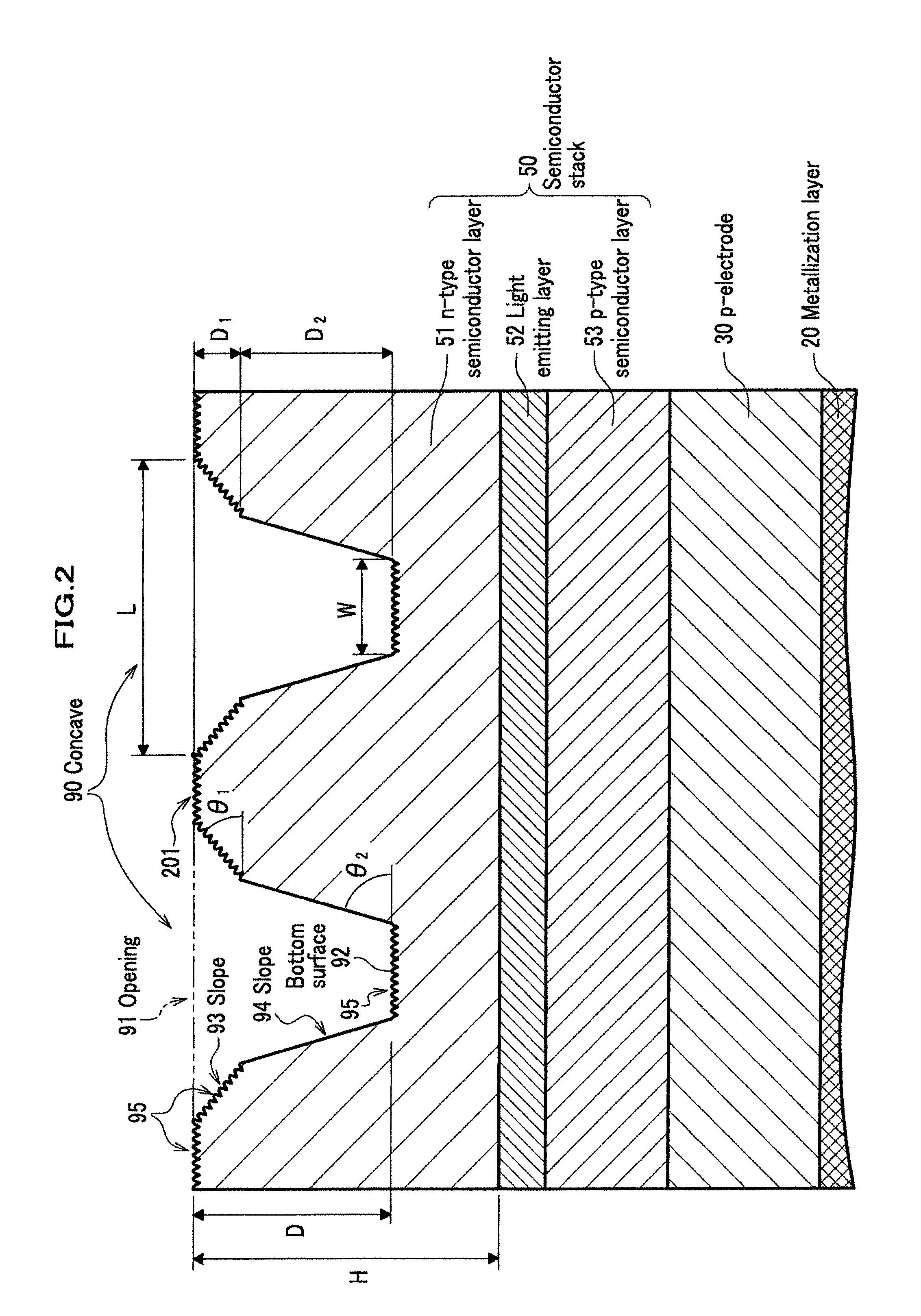
[0135]FIG. 13 is a view schematically showing a plane, X-X cross section and Y-Y cross section of a first modified example of an opening of a concave, and FIG. 14 is a perspective view schematically showing a partial cross section of the first modified example taken along Y-Y cross section shown in FIG. 13. In the first modified example, a configuration of the opening is the same as that of concave 90 shown in FIG. 3 except that a shape of a plurality of concave openings is a hexagon and that a density of the concave opening is not so high as shown in FIG. 3. Namely, for example, in the concave 90a, each vertex of the regular hexagon as an opening is in contact with six concaves 90b to 90g surrounding the concave 90a. In other words, the concave 90a is surrounded by six regular triangles shown in plane view of FIG. 13. These six triangles are located on the light extraction surface. Therefore, a current diffusion on the light extraction surface becomes good. It is noted that each ve...
second modified example
[0136]FIG. 15 is a view schematically showing a plane, X-X cross section and Y-Y cross section of a second modified example of an opening of a concave, and FIG. 16 is a perspective view schematically showing a partial cross section of the second modified example taken along Y-Y cross section shown in FIG. 15. In the second modified example, an arrangement of openings of a plurality of concaves is shown in FIG. 15, which is a close-packed structure. Namely, for example, the concave 90a is in contact with six surrounding concaves by respective sides of a regular hexagon as an opening. In addition, the concave 90a is in contact with six surrounding concaves at respective vertexes of the regular hexagon as an opening. Here, as shown in FIG. 16 which is a Y-Y arrow cross section of FIG. 15, for example, each side of the regular hexagon as an opening of the concave 90a is straight and on the light extraction surface. As described above, in the second modified example, each side and each v...
third modified example
[0137]FIG. 17 is a view schematically showing a plane, X-X cross section and Y-Y cross section of a third modified example of an opening of a concave, and FIG. 18 is a perspective view schematically showing a partial cross section of the third modified example taken along Y-Y cross section of FIG. 17. In the third embodiment, each side of a regular hexagon as an opening of the concave 90a is not a straight line, but a v-shaped line having a vertex (bottom) at the center of the side. Namely, only respective vertexes of the regular hexagon in plane view are located on a plane identical to the light extraction surface. Here, an upper slope (slope 93, see FIG. 2) is located below a valley of the V-shape. In other words, the V-shape is within the upper slope (slope 93, see FIG. 2). Therefore, there is an advantage that a current can be easily and uniformly diffused in comparison with a case where the v-shape is not formed. Other characteristics are the same with those of the second modif...
PUM
 Abstract
Description
Claims
Application Information