Light emitting element and light emitting device
a technology of light emitting elements and light emitting devices, which is applied in the direction of basic electric elements, semiconductor devices, electrical equipment, etc., can solve the problems of increasing drive voltage, increasing drive voltage, and required to greatly decrease, and achieves high current density distribution, and further improved light extraction efficiency
- Summary
- Abstract
- Description
- Claims
- Application Information
AI Technical Summary
Benefits of technology
Problems solved by technology
Method used
Image
Examples
exemplary embodiment 1
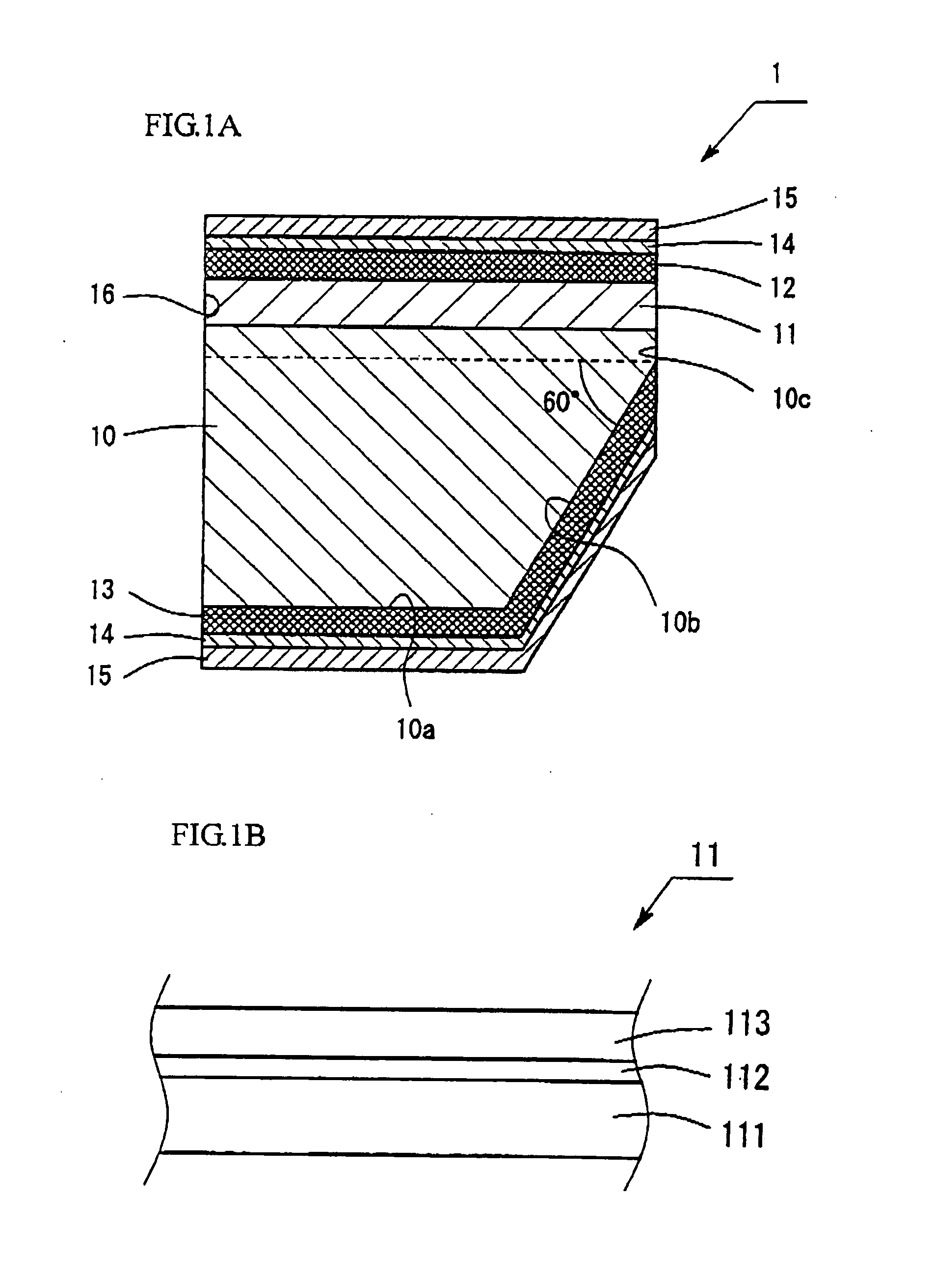
[0058]FIG. 1 is a view showing the structure of a light emitting element 1 of an exemplary embodiment 1. The light emitting element 1 includes an n-GaN substrate 10, a semiconductor layer 11 made of group III nitride semiconductor stacked on the surface of the n-GaN substrate 10, a p electrode 12 formed on the entire surface 11a of the semiconductor layer 11, and an n electrode 13 formed on a back surface (second surface) 10a of the n-GaN substrate 10. Also, the plane shape of the light emitting element 1 is rectangular, in which the long side is 1000 μm, the short side is 300 μm, and the area is 0.3 mm2. FIG. 1A shows the cross-section in the short side direction, in which the long side direction is the direction perpendicular to the paper surface in FIG. 1A.
[0059]The semiconductor layer 11 has a structure in which an n layer 111, an active layer 112 and a p layer 113 are stacked in this order, as shown in FIG. 1B. The n layer 111 has a structure in which an n-type contact layer ma...
exemplary embodiment 2
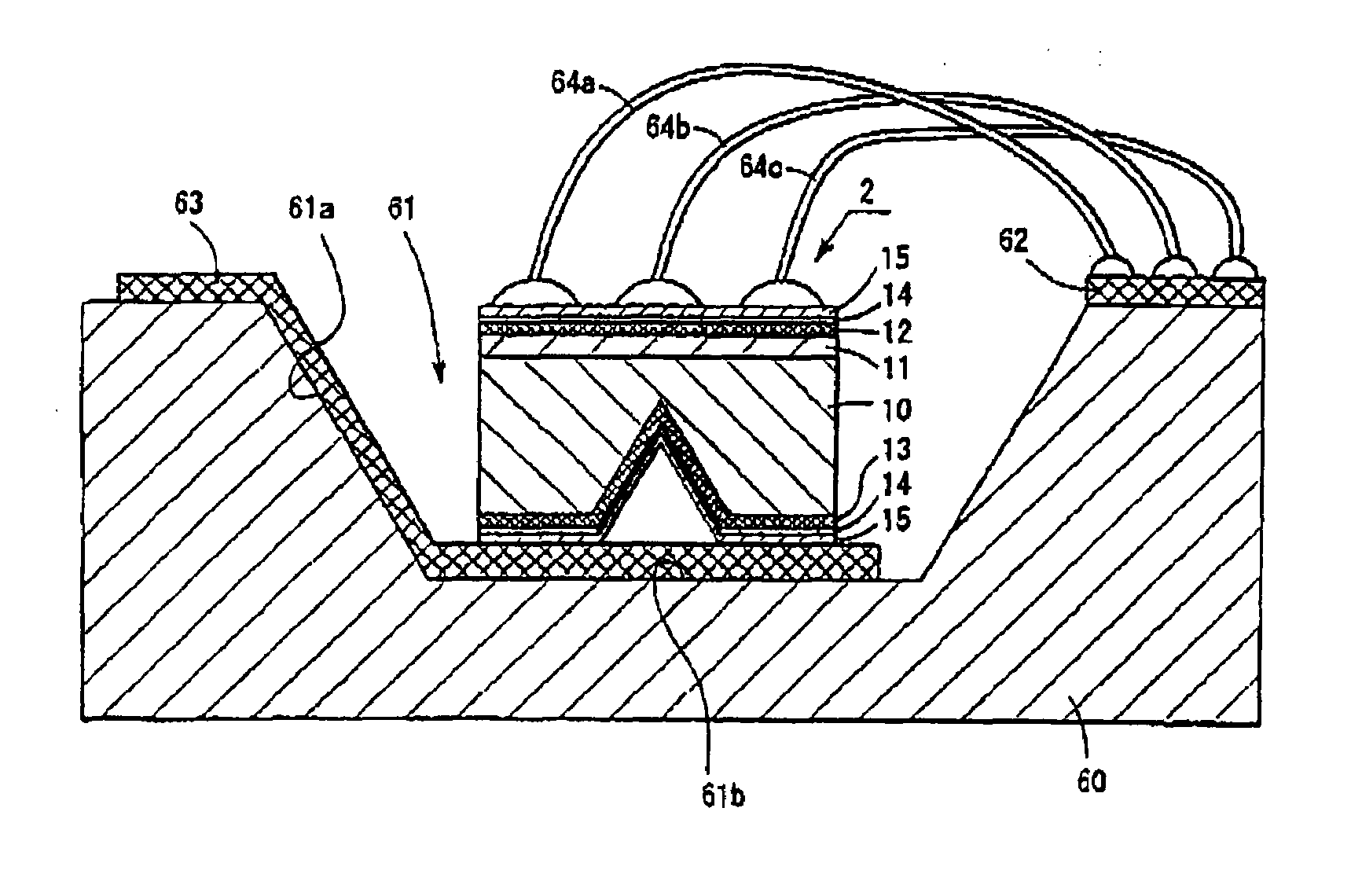
[0075]FIG. 7 shows a structure of a light emitting element 2 of an embodiment 2. This light emitting element 2 includes the semiconductor layer 11, the p electrode 12 and the n electrode 13 on the surface of an n-GaN substrate 20 in the same way as the light emitting element 1 of the embodiment 1. A difference from the light emitting element 1 of the embodiment 1 is that the worked shape of a back surface 20a of the n-GaN substrate 20 is different from the worked shape of the n-GaN substrate 10 in the embodiment 1. That is, it is different in that a concave portion 21 in the shape of V character with a tapered surface 20b inclined to the n-GaN substrate 20 as the lateral surface is formed in the central part of the back surface 20a of the n-GaN substrate 20. It is desirable that the thickness d from the position of a vertex angle of the V character to the semiconductor layer is in the range from 30 to 60% of the thickness of the n-GaN substrate 20. Also, it is desirable that the ang...
PUM
 Abstract
Description
Claims
Application Information


