Circuit device

a circuit device and circuit technology, applied in the field of circuit devices, can solve the problems of inability to achieve the miniaturization of the device in total size, the temperature of the junction thereof is higher than the temperature, etc., and achieve the effect of suppressing thermal interference and suppressing overheating of semiconductor elements

Active Publication Date: 2010-04-01
SEMICON COMPONENTS IND LLC
View PDF6 Cites 13 Cited by
  • Summary
  • Abstract
  • Description
  • Claims
  • Application Information

AI Technical Summary

Benefits of technology

[0011]According to the present invention, when semiconductor elements fixed to heat spreaders are arranged close to each other, the semiconductor elements are mounted on upper surfaces of the heat spreaders at positions offset from each other. Accordingly, the semiconductor elements fixed to the respective upper surfaces of the heat spreaders arranged close to each other can be spaced apart from one another as far as possible. Hence, thermal interference is suppressed and thus overheating of the semiconductor elements is suppressed.

Problems solved by technology

However, when multiple power transistors are arranged in a small region for the purpose of miniaturization of the entire device incorporating, for example, an inverter circuit, these transistors thermally interfere with each other, and thereby cause a problem that the junction temperature thereof becomes higher than the temperature caused by self-heating.
In contrast, when transistors are arranged to be spaced apart from each other in order to avoid the above problem, another problem arises that miniaturization of the device in total size cannot be achieved even though thermal interference is suppressed.

Method used


Image

  • Circuit device
  • Circuit device
  • Circuit device

Examples


Embodiment Construction

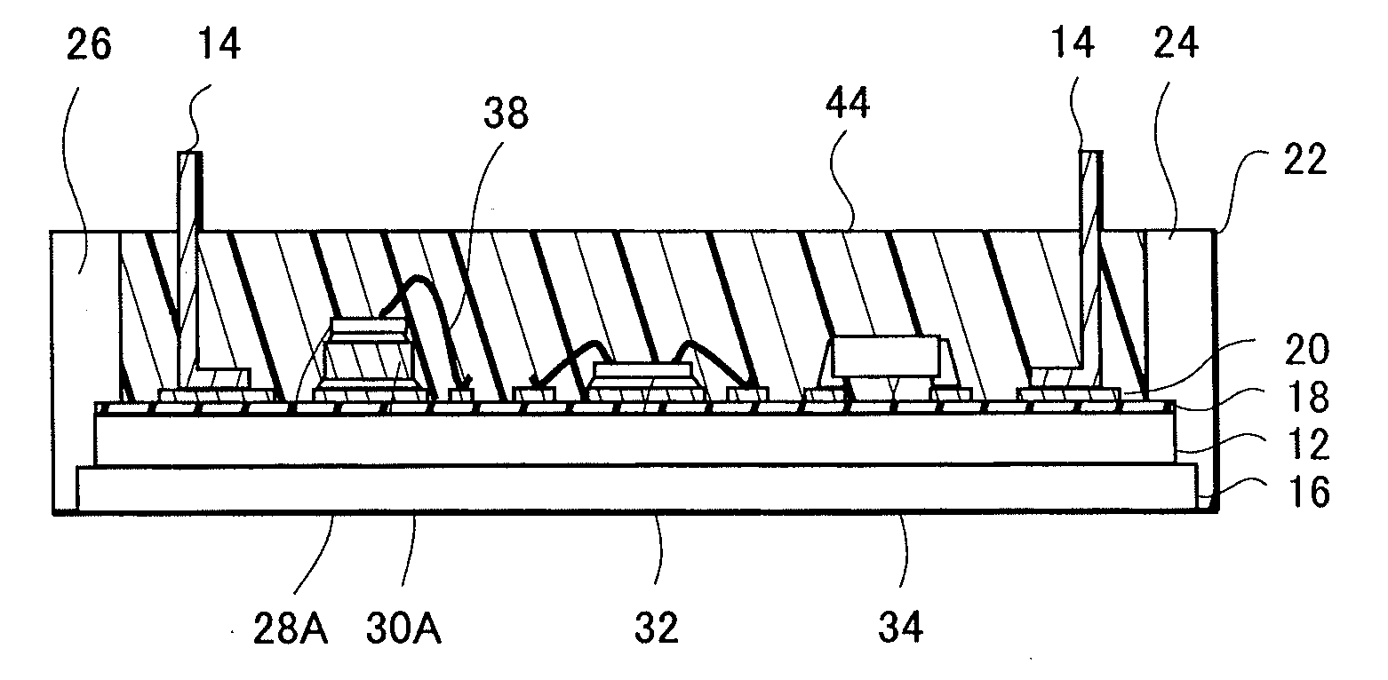
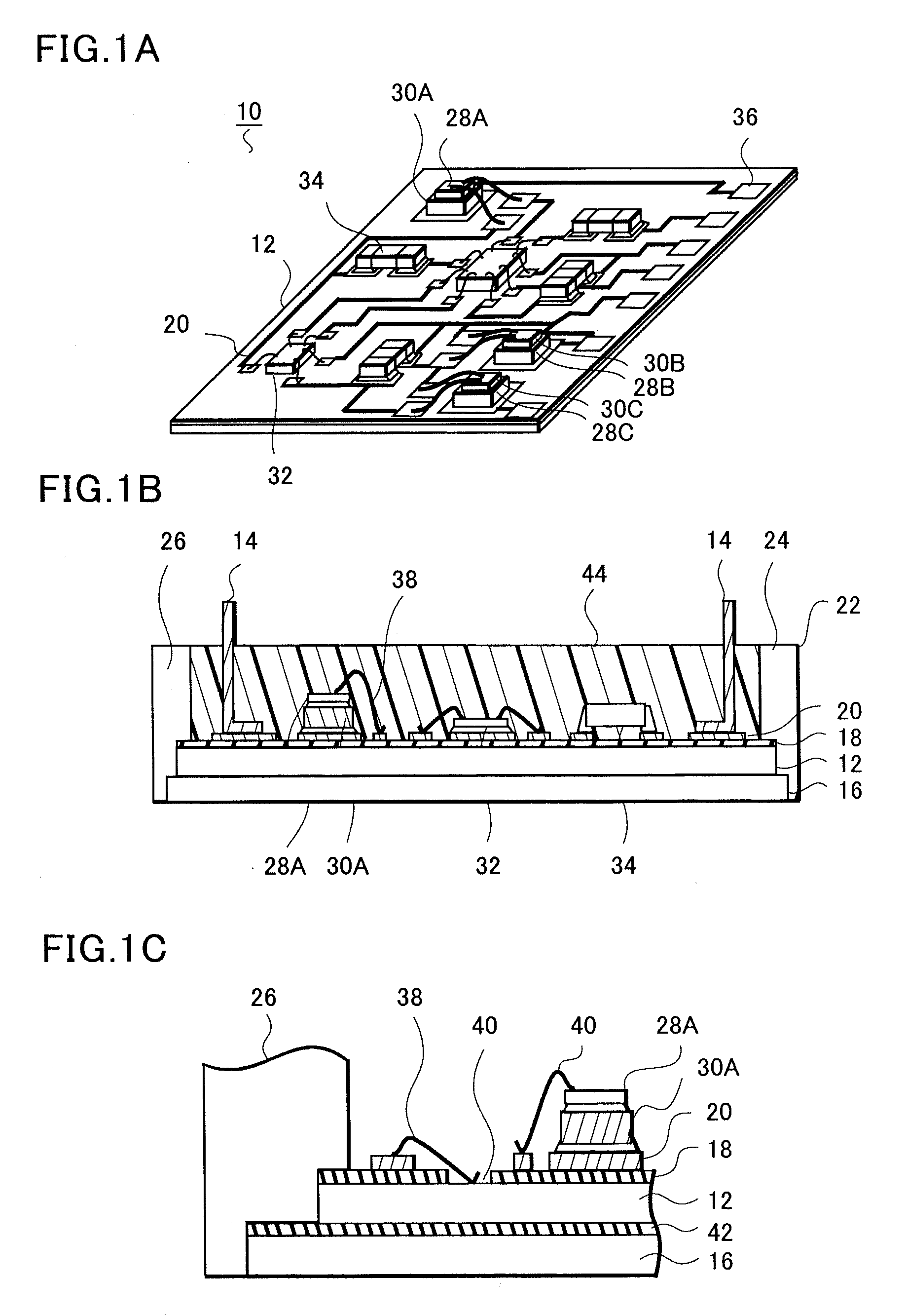
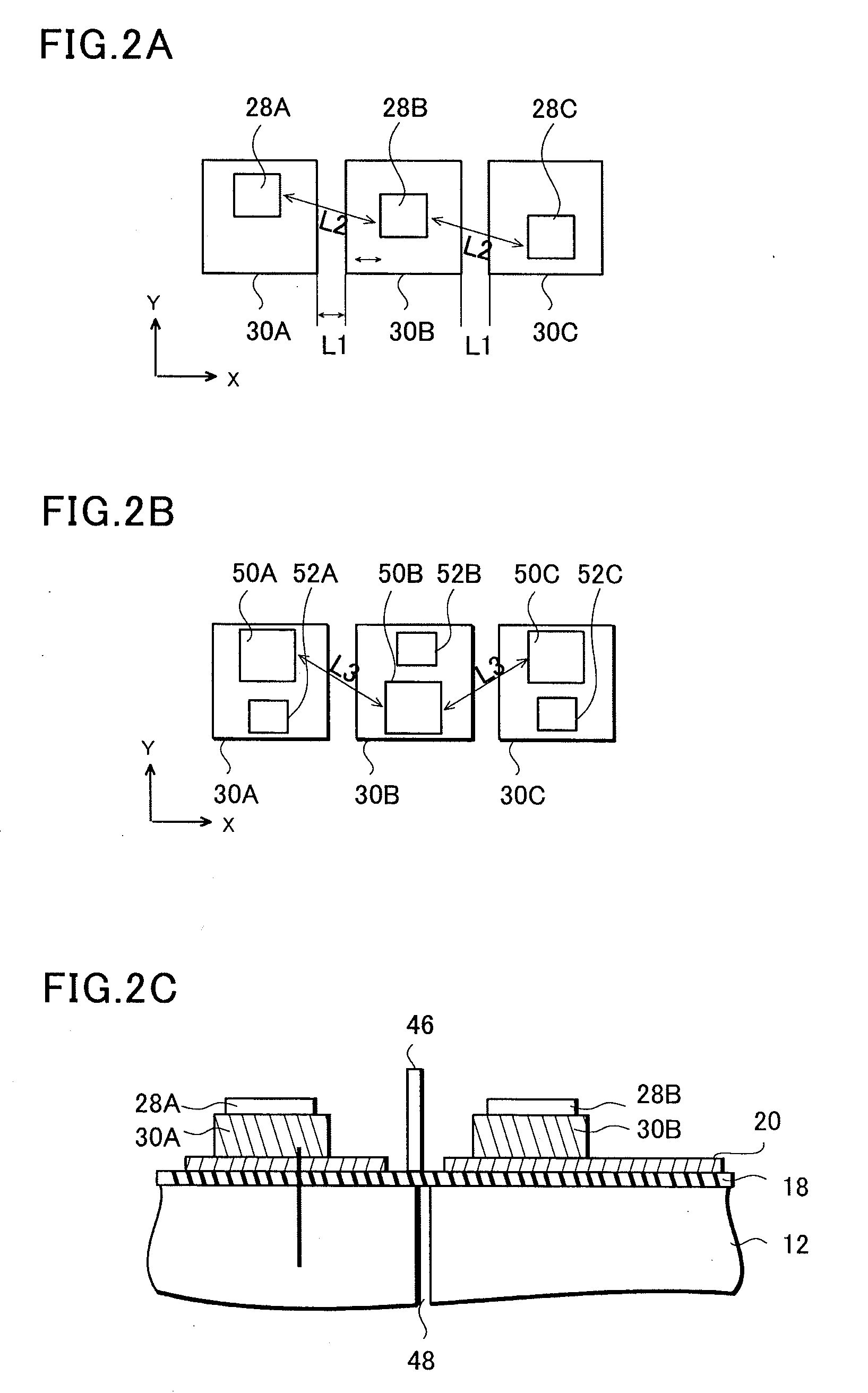
[0017]With reference to FIGS. 1A to 1C, a description will be given of a configuration of a hybrid integrated circuit device 10 as an example of a circuit device of the present invention. FIG. 1A is a perspective view for illustrating the hybrid integrated circuit device 10; FIG. 1B is a representative cross-sectional view of the hybrid integrated circuit device 10; and FIG. 1C is an enlarged cross-sectional view thereof.

[0018]As shown in FIGS. 1A and 1B, the hybrid integrated circuit device 10 mainly includes: a circuit substrate 12 incorporated with a hybrid integrated circuit in its upper surface; a sealing resin 44 for sealing the hybrid integrated circuit by coating the circuit substrate 12; and leads 14 extending to the outside while being fixed to pads formed of the conductive pattern 20. Here, the hybrid integrated circuit is formed of a conductive pattern 20, and semiconductor elements 28A and so on (circuit elements).

[0019]The circuit substrate 12 is a metal substrate main...


PUM


Abstract

Provided is a circuit device having a configuration in which thermal interference between built-in elements is suppressed and being miniaturized in total size. A hybrid integrated circuit device of the present invention includes: a circuit substrate, a sealing resin and leads. The circuit substrate in its upper surface is incorporated with a hybrid integrated circuit formed of semiconductor elements and the like respectively fixed to heat spreaders. The sealing resin coats the circuit substrate and thus seals the hybrid integrated circuit. The leads each extend to the outside while being fixed to a pad formed of a conductive pattern. In this hybrid integrated circuit device, the semiconductor elements are mounted on the respective heat spreaders at positions offset from each other, and thereby are arranged to be spaced away from each other.

Description

[0001]This application claims priority from Japanese Patent Application Number JP 2008-250914 filed on Sep. 29, 2008, the content of which is incorporated herein by reference in its entirety.BACKGROUND OF THE INVENTION[0002]1. Field of the Invention[0003]The present invention relates to a circuit device, and particularly to a circuit device in which thermal interference between elements is suppressed.[0004]2. Description of the Related Art[0005]With reference to FIG. 5, a description will be given of a configuration of a hybrid integrated circuit device 100 as an example of a conventional circuit device. Firstly, a conductive pattern 103 is formed on a surface of a rectangular substrate 101 with an insulating layer 102 interposed therebetween. Circuit elements are fixed to desired portions of the conductive pattern 103, and thereby a predetermined electrical circuit is formed. Herein, a semiconductor element 105A and a chip element 105B are employed as the circuit elements. The semi...

Claims


Application Information

Patent Timeline
Patent Type & Authority Applications(United States)
IPC IPC(8): H01L27/06
CPCH01L23/24H01L2924/3025H01L25/18H01L2924/13055H01L2924/13091H01L24/48H01L2224/32225H01L2224/48227H01L2224/73265H01L2924/19105H01L25/072H01L2924/30107H01L2924/19107H01L2224/49111H01L2224/48472H01L2224/48091H01L2924/1305H01L2924/00H01L2924/00012H01L2924/00014H01L2224/451H01L2224/45015H01L24/45H01L2924/181H01L24/73H01L2924/14H01L2224/48139H01L24/49H01L2924/00015H01L2924/2076H01L2224/05599
Inventor KUDO, KIYOAKISHIBASAKI, TAKASHIYAMAMOTO, TETSUYA
Owner SEMICON COMPONENTS IND LLC
Why Eureka
Try Eureka