Methods for fabricating large area nanoimprint molds

a nanoimprint mold and large area technology, applied in the field of large area nanoimprint mold fabrication, can solve the problems of inability to meet current needs, inability to meet current fabrication requirements, and significant reduction in fabrication reliability and throughput, and achieve the effect of avoiding the use of large-area sers and reducing the number of manufacturing steps

Active Publication Date: 2010-04-01
CHOU +3
View PDF13 Cites 11 Cited by
  • Summary
  • Abstract
  • Description
  • Claims
  • Application Information

AI Technical Summary

Problems solved by technology

The current fabrication approaches cannot meet current needs.
However, as the feature size gets below 30 nm, not all EBL tools and processes can be used, and the fabrication reliability and throughput are significantly reduced.
Clearly this method is impractical for large-area SERS applications.
Nanosphere lithography has the capability to pattern large areas efficiently, however the controllability and reliability of the pattern positioning are poor.
Furthermore the only a limited range of geometric profiles can be patterned by nanosphere lithography.

Method used


Image

  • Methods for fabricating large area nanoimprint molds
  • Methods for fabricating large area nanoimprint molds
  • Methods for fabricating large area nanoimprint molds

Examples


Embodiment Construction

[0019]Nanofabrication with Fine Feature Size, High Precision and Fast Turnaround

[0020]To meet the needs of high resolution and fast turnaround nanopatterning for

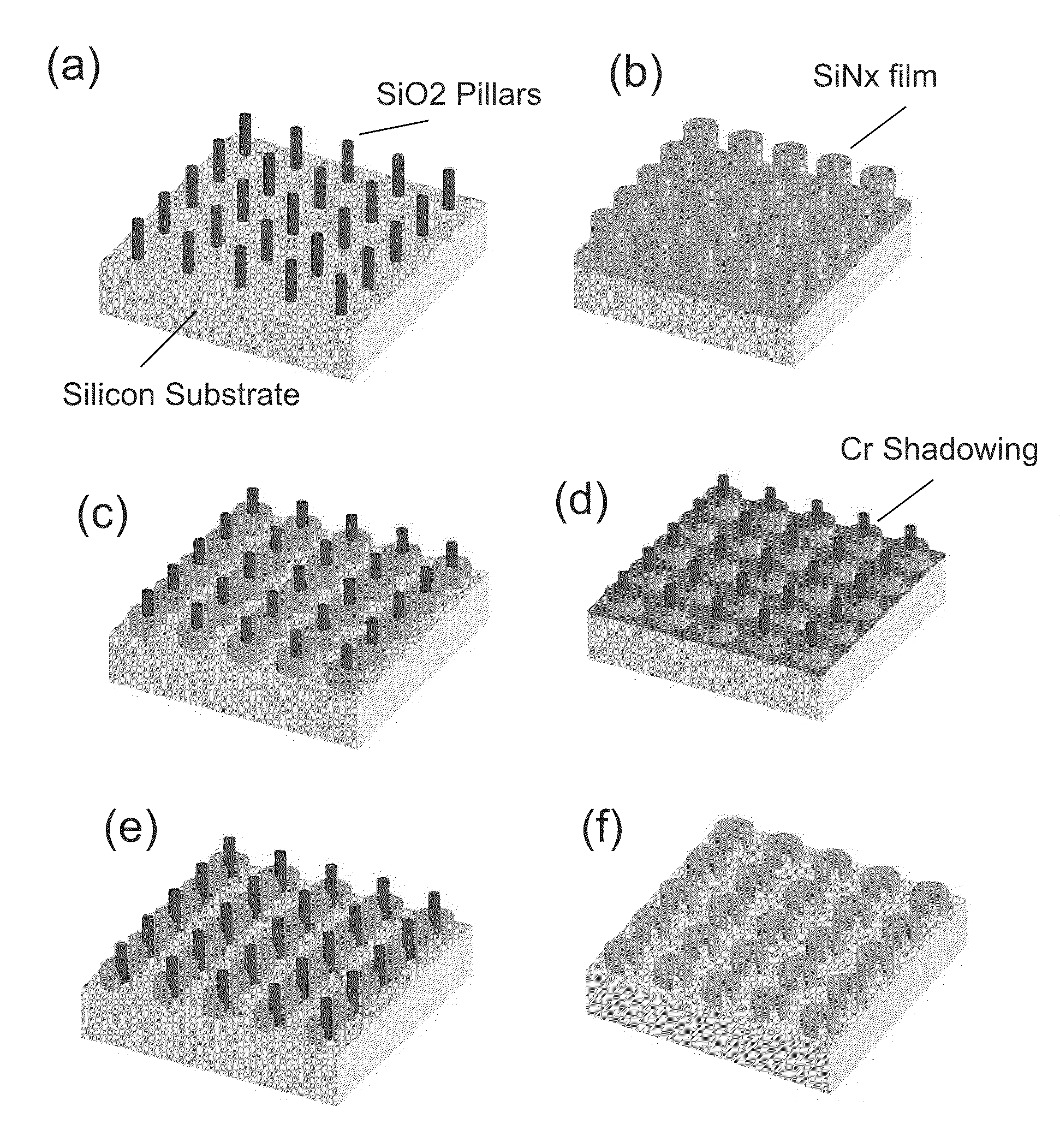
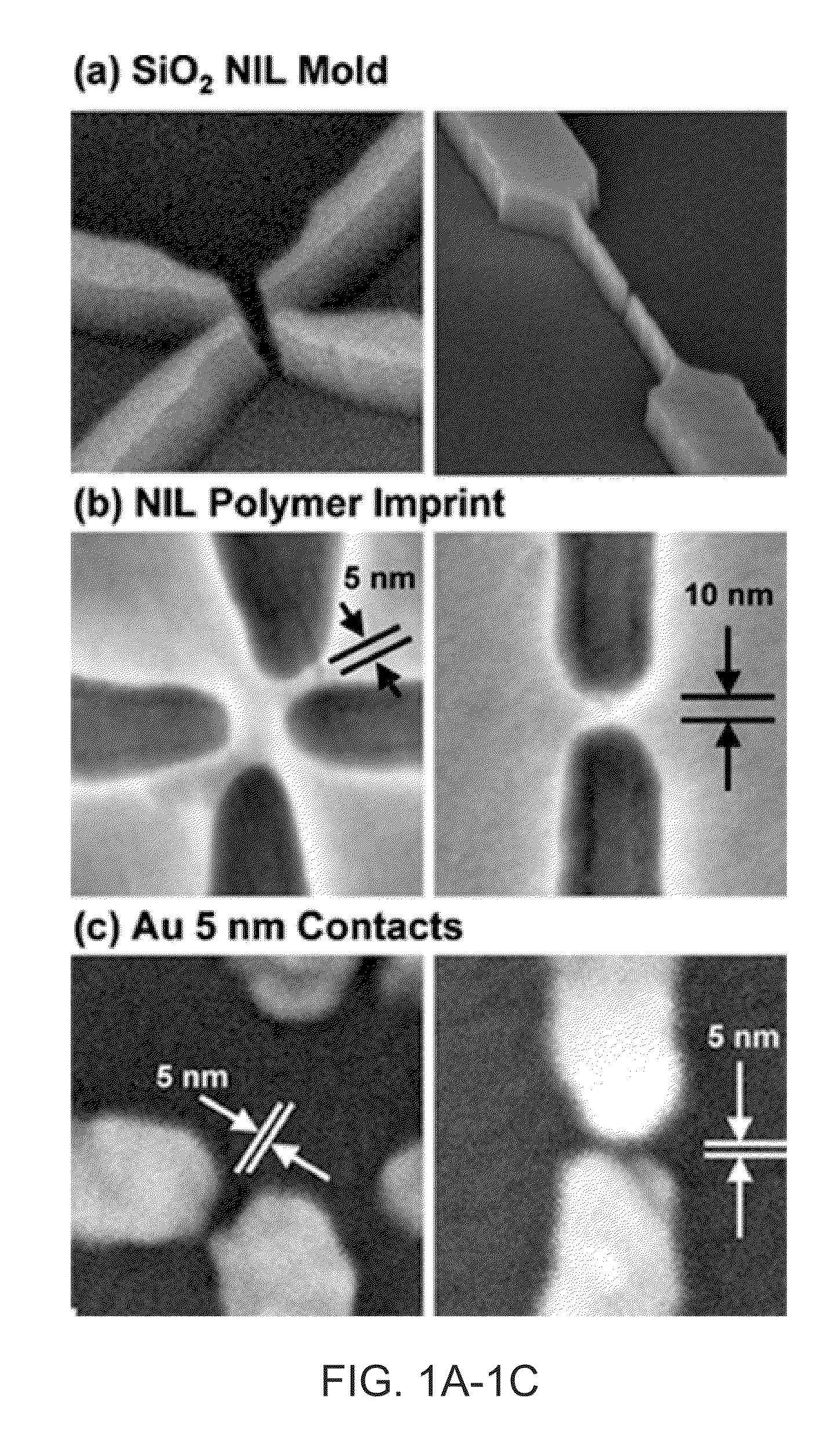
[0021]SERS research and applications, we propose the use nanoimprint as a major approach to duplicate the SERS patterns with molds fabricated by either direct writing or by other innovative methods that do not need direct writing. Our innovative methods can create SERS nanoimprint molds over large areas (6″ wafers), and can create very small feature sizes with good dimension control.

[0022]The reason for avoiding direct-write EBL in producing SERS nanostructures is that as the feature size becomes smaller, the reliability and dimension control of EBL becomes very poor and throughput drops drastically. Hence, multiple runs are required to obtain one good sample. In contrast , once a good nanoimprinting mold is made (the original or “master” mold), each NIL duplication will faithfully reproduce the exact pattern on the mold wit...


PUM

PropertyMeasurementUnit
sizeaaaaaaaaaa
areaaaaaaaaaaa
diameteraaaaaaaaaa

Abstract

This invention relates to the fabrication of large area nanoimprint molds having complex patterns with minimal or no use of direct-writing, such as electron beam lithography, ion, laser beam, or mechanical beam lithography. This can be accomplished by forming a pattern of simple nanoscale features and converting the simple features into more complex nanoscale features by a process comprising shadow deposition. The process may also include steps of uniform deposition, etching and smoothing depending on the shape of the complex features.

Description

CROSS-REFERENCE TO RELATED APPLICATIONS[0001]This application claims the benefit of Provisional Application No. 61 / 056,319 filed on May 27, 2008, which is incorporated herein by reference. This application is also related to U.S. application Ser. No. 10 / 140,140 filed May 7, 2002, (now U.S. Pat. No. 7,137,803, issued to Stephen Y. Chou on Nov. 21, 2006) and to U.S. application Ser. No. 11 / 442,900 filed on May 29, 2006 (now U.S. Pat. No. 7,282,456 issued to Stephen Y. Chou, et al. on Oct. 16, 2007), both of which are herein incorporated by reference.STATEMENT REGARDING FEDERALLY SPONSORED RESEARCH[0002]Not Applicable.BACKGROUND OF THE INVENTION[0003]This invention relates to the fabrication of large area nanoimprint molds with complex patterns with minimal or no use of direct-writing, such as electron beam lithography, ion, laser beam, or mechanical beam lithography.[0004]The key challenges in the fabrication of Surface-Enhanced Raman Scattering[0005](SERS) nanostructures for research...

Claims


Application Information

Patent Timeline
Patent Type & Authority Applications(United States)
IPC IPC(8): B29C59/02
CPCB82Y10/00G03F7/0002B82Y40/00Y10S977/887
Inventor CHOU, STEPHEN Y.CAN, PENGLI, WENDIBAI, SHUFUNG
Owner CHOU
Why Eureka
Try Eureka