Method for forming self-aligned dielectric cap above floating gate

a dielectric cap and floating gate technology, applied in the direction of semiconductor devices, basic electric elements, electrical appliances, etc., can solve the problems of increasing the difficulty of leakage current, and increasing the leakage current, so as to reduce the leakage current and reduce the strength of the electric field

Active Publication Date: 2010-04-01
SANDISK TECH LLC
View PDF30 Cites 17 Cited by
  • Summary
  • Abstract
  • Description
  • Claims
  • Application Information

AI Technical Summary

Benefits of technology

[0017]Embodiments in accordance with the disclosure, roughly described, pertain to techniques for fabricating memory cells and memory arrays. The memory cell has a dielectric cap above a floating gate. In one embodiment, the dielectric cap resides between the floating gate and a conformal IPD layer. The dielectric cap reduces the leakage current between the floating gate and a control gate. The dielectric cap achieves this reduction by reducing the strength of the electric field at the top of the floating gate, which is where the electric field would be strongest without the dielectric cap for a floating gate having a narrow stem.

Problems solved by technology

However, it is possible for charge to leak through the inter-poly dielectric from the floating gate to the control gate, which is referred to as leakage current.
However, if the IPD is too thin, the leakage current can become undesirably large.
As non-volatile memory structures become smaller, leakage current is becoming a more difficult problem.
One reason for the leakage current problem is the strength of the electric field that occurs in various portions of the IPD when a voltage is applied to the control gate.
In particular, the electric field is enhanced in certain regions of the IPD, which results in greater leakage current.
Therefore, as feature sizes of memory cells continue to be reduced, the electric field in the IPD 106 and hence leakage current becomes more difficult to deal with.
However, such films are difficult to work with and hence undesirable.
For example, paraelectric materials have dielectric constants that are usually at least two orders of magnitude above that of silicon dioxide, but several problems limit their use as gate dielectrics.
One such problem is oxygen diffusion.
However, because the deposited high dielectric metal oxides have non-stoichiometric composition, they are prone to large electrical defects or traps in the bulk of the dielectric and at the dielectric / semiconductor interface.
These defects or traps enhance conduction through the dielectric and reduce the breakdown strength of the dielectric.
However, increasing the thickness of the IPD 106 tends to reduce the capacitive coupling between the floating gate 102 and the control gate 106, which is undesirable for reasons previously discussed.

Method used


Image

  • Method for forming self-aligned dielectric cap above floating gate
  • Method for forming self-aligned dielectric cap above floating gate
  • Method for forming self-aligned dielectric cap above floating gate

Examples


Embodiment Construction

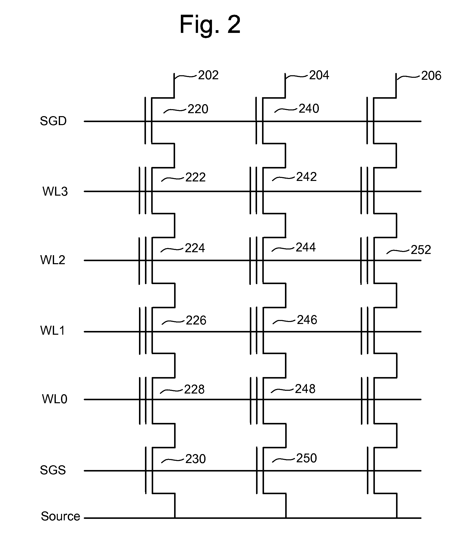
[0035]One example of a flash memory system uses the NAND structure, which includes arranging multiple floating gate transistors in series between two select gates. The transistors in series and the select gates are referred to as a NAND string. A typical architecture for a flash memory system using a NAND structure will include several NAND strings. For example, FIG. 2 shows three NAND strings 202, 204 and 206 of a memory array having many more NAND strings. Each of the NAND strings of FIG. 2 includes two select transistors and four memory cells. For example, NAND string 202 includes select transistors 220 and 230, and memory cells 222, 224, 226 and 228. NAND string 204 includes select transistors 240 and 250, and memory cells 242, 244, 246 and 248. Each NAND string is connected to the source line by its select transistor (e.g. select transistor 230 and select transistor 250). A selection line SGS is used to control the source side select gates. The various NAND strings are connecte...


PUM


Abstract

A method for fabricating a non-volatile storage element. The method comprises forming a layer of polysilicon floating gate material over a substrate and forming a layer of nitride at the surface of the polysilicon floating gate material. Floating gates are formed from the polysilicon floating gate material. Individual dielectric caps are formed from the nitride such that each individual nitride dielectric cap is self-aligned with one of the plurality of floating gates. An inter-gate dielectric layer is formed over the surface of the dielectric caps and the sides of the floating gates. Control gates are then formed with the inter-gate dielectric layer separating the control gates from the floating gates. The layer of nitride may be formed using SPA (slot plane antenna) nitridation. The layer of nitride may be formed prior to or after etching of the polysilicon floating gate material to form floating gates.

Description

CROSS-REFERENCE TO RELATED APPLICATIONS[0001]The following applications are cross-referenced and incorporated by reference herein in their entirety:[0002]U.S. patent application Ser. No. 12 / 170,321, entitled “METHOD OF FORMING DIELECTRIC LAYER ABOVE FLOATING GATE FOR REDUCING LEAKAGE CURRENT,” by James Kai, et al., filed on Jul. 9, 2008; and[0003]U.S. patent application Ser. No. 12 / 170,327, entitled “DIELECTRIC LAYER ABOVE FLOATING GATE FOR REDUCING LEAKAGE CURRENT,” by Dana Lee, et al., filed on Jul. 9, 2008.BACKGROUND OF THE INVENTION[0004]1. Field of the Invention[0005]The present invention relates to non-volatile memory devices.[0006]2. Description of the Related Art[0007]Semiconductor memory devices have become more popular for use in various electronic devices. For example, non-volatile semiconductor memory is used in cellular telephones, digital cameras, personal digital assistants, mobile computing devices, non-mobile computing devices and other devices. Electrical Erasable ...

Claims


Application Information

Patent Timeline
Patent Type & Authority Applications(United States)
IPC IPC(8): H01L21/3205
CPCH01L21/28273H01L27/11519H01L29/7881H01L29/513H01L27/11521H01L29/40114H10B41/10H10B41/30
Inventor PURAYATH, VINOD ROBERTMATAMIS, GEORGEORIMOTO, TAKASHICHIEN, HENRYKAI, JAMES K.
Owner SANDISK TECH LLC
Why Eureka
Try Eureka