Semiconductor diode with reduced leakage

a technology of silicon based ics and diodes, applied in the direction of diodes, semiconductor devices, semiconductor/solid-state device details, etc., can solve the problems of catastrophic damage to the integrated circuit, the thinnest dielectric layer fails at lower voltage, and the silicon based ics are particularly susceptible to electrostatic discharge damage, etc., to achieve the effect of reducing the reverse leakage curren

Inactive Publication Date: 2005-02-17
TAIWAN SEMICON MFG CO LTD
View PDF77 Cites 155 Cited by
  • Summary
  • Abstract
  • Description
  • Claims
  • Application Information

AI Technical Summary

Benefits of technology

[0007] The present invention provides a semiconductor diode for electrostatic discharge protection that is compatible with the fabrication processes of advanced transistors and has reduced reverse leakage current.

Problems solved by technology

These thinner dielectric layers fail at lower voltages.
These types of failures are a major concern in advanced semiconductor technology.
Silicon based ICs are particularly susceptible to electrostatic discharge damage, for example in the situation where a user of a device containing an integrated circuit develops a static charge on their body and subsequently comes in contact with the device containing the integrated circuit.
Such a high instantaneous voltage may catastrophically damage the integrated circuit.

Method used


Image

  • Semiconductor diode with reduced leakage
  • Semiconductor diode with reduced leakage
  • Semiconductor diode with reduced leakage

Examples


Embodiment Construction

[0024] The making and using of the presently preferred embodiments are discussed in detail below. It should be appreciated, however, that the present invention provides many applicable inventive concepts that can be embodied in a wide variety of specific contexts. The specific embodiments discussed are merely illustrative of specific ways to make and use the invention, and do not limit the scope of the invention.

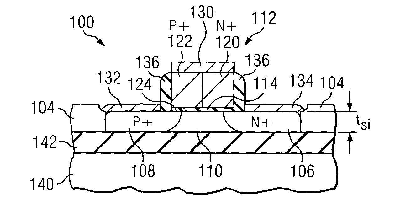
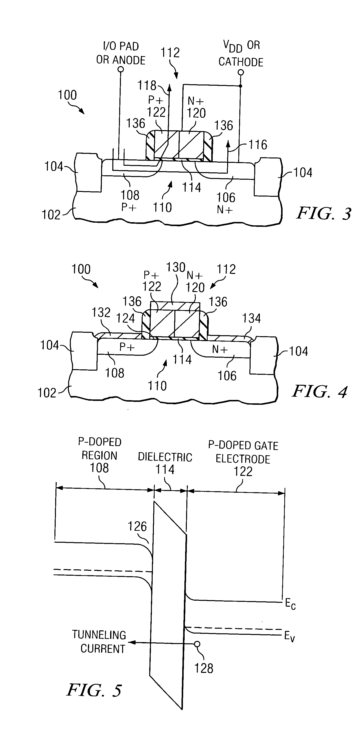
[0025] The present invention will be described with respect to preferred embodiments in a specific context, namely a gated diode for use in protecting semiconductor devices from electrostatic discharge damage. The invention may also be applied, however, to other semiconductor components for which reduced leakage current is a desirable design goal.

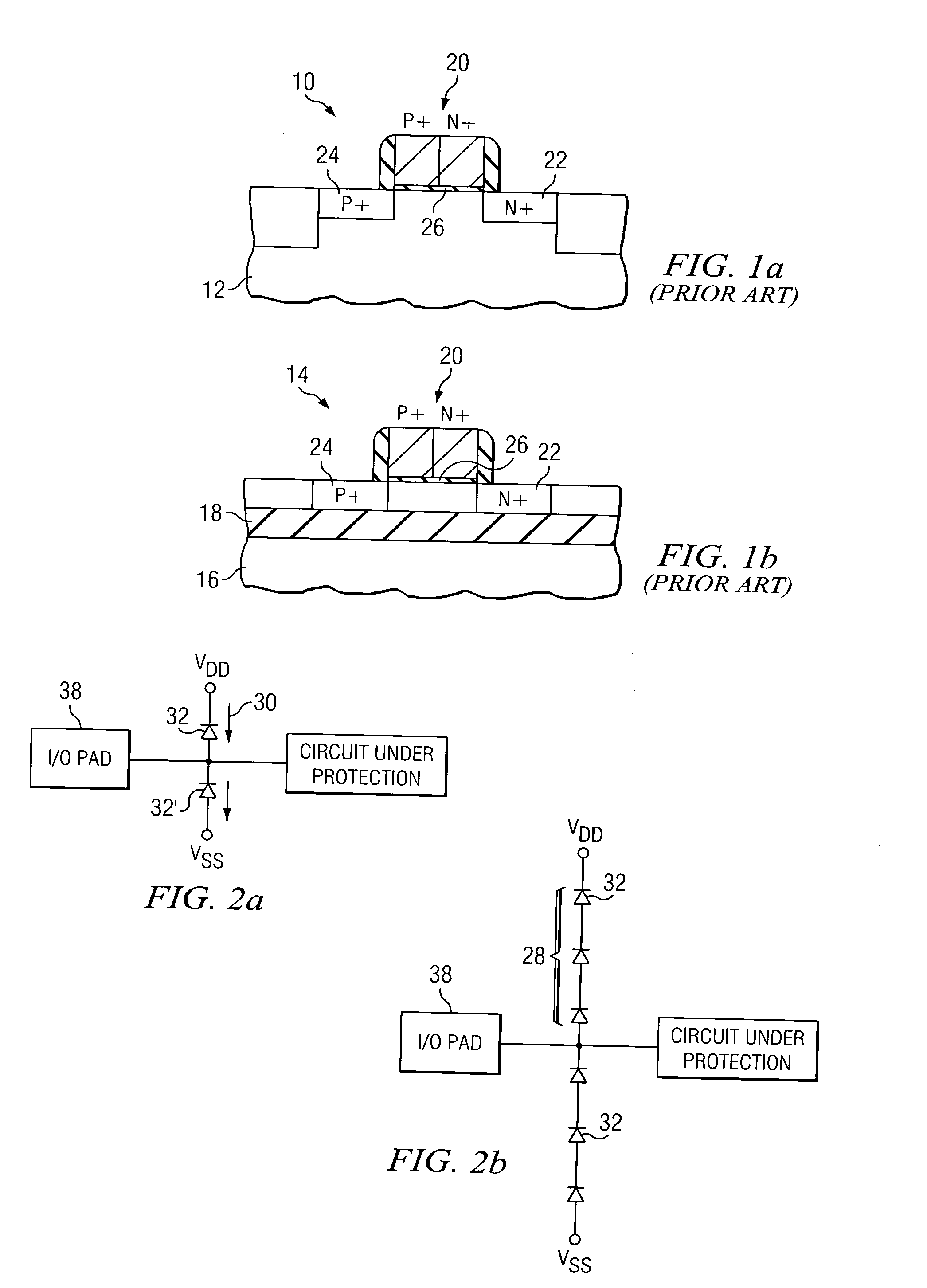
[0026] As will be discussed in greater detail below, the preferred embodiment of the present invention relates to a diode that has reduced leakage. FIGS. 2a and 2b illustrate how these diodes can be used in for electrostatic disch...


PUM


Abstract

A diode 100 is formed on a silicon-on-insulator substrate that includes a silicon layer overlying an insulator layer 142. An active region is formed in the silicon layer and includes a p-doped region 108 and an n-doped region 106 separated by a body region 110. A high permittivity gate dielectric 114 overlies the body region 110 and a gate electrode 112 overlies the gate dielectric 114. As an example, the diode can be used for ESD protection.

Description

TECHNICAL FIELD [0001] The present invention relates to the field of semiconductor devices, and more specifically, to a semiconductor diode device for electrostatic discharge protection in advanced complementary metal-oxide-semiconductor (CMOS) technologies. BACKGROUND [0002] Transistor size reduction has resulted in the thinning of insulator layers such as the gate dielectric. These thinner dielectric layers fail at lower voltages. Consequently, device scaling increases circuit sensitivity to voltage stress, electrical overstress (EOS), and electrostatic discharge (ESD). These types of failures are a major concern in advanced semiconductor technology. This is especially true for integrated circuit (IC) chips that interface with other chips or signals with voltages above that of the IC chip itself. [0003] Silicon based ICs are particularly susceptible to electrostatic discharge damage, for example in the situation where a user of a device containing an integrated circuit develops a ...

Claims


Application Information

Patent Timeline
Patent Type & Authority Applications(United States)
IPC IPC(8): H01L21/84H01L27/06H01L27/08H01L27/12H01L29/49H01L29/739
CPCH01L21/84H01L27/0629H01L29/7392H01L27/1203H01L29/4983H01L27/0814
Inventor YEO, YEE-CHIAYANG, FU-LIANGHU, CHENMING
Owner TAIWAN SEMICON MFG CO LTD
Why Eureka
Try Eureka