Light emitting diode package and fabricating method thereof

a technology of light-emitting diodes and led packages, which is applied in the manufacture of semiconductor/solid-state devices, electrical devices, and semiconductor devices. it can solve the problems of high manufacturing cost, easy damage to bonding wires b>150/b>, and increase manufacturing costs. , to achieve the effect of reducing fabrication costs, avoiding damage to bonding wires, and increasing the yield rate of led packages

Inactive Publication Date: 2010-04-08
NOVALITE OPTRONICS CORP
View PDF3 Cites 36 Cited by
  • Summary
  • Abstract
  • Description
  • Claims
  • Application Information

AI Technical Summary

Benefits of technology

[0008]The present application is directed to an LED package having apertures for accommodating devices. The LED package of the present application is capable of avoiding damage of bonding wires such that the yield rate of the LED package is increased and the fabrication cost is reduced.
[0009]The present application is directed to a method of fabricating an LED package, which has simpler fabricating processes and is advantage in reduced fabrication cost.
[0035]In the LED package of the present application, a first aperture and a second aperture are formed to improve damage issue of bonding wires. Accordingly, amount of the material required for fabricating the package housing and the fabrication cost is reduced. In addition, the yield rate of the LED package is increased enhanced, since the physical strength of the carrier is enhanced by the strength enhancement structure.

Problems solved by technology

However, since the bonding wires 150 electrically connected with the ESD protector 140 are encapsulated by the package housing 120, the bonding wires 150 electrically connected with the ESD protector 140 are damaged easily during fabrication.
Specifically, the bonding wires 150 may be damaged by liquid molding compound when a mold injection process is performed to form the package housing 120.
However, the fabrication cost increases significantly because the surface mount technology (SMT) is much more complex than wire bonding process.

Method used


Image

  • Light emitting diode package and fabricating method thereof
  • Light emitting diode package and fabricating method thereof
  • Light emitting diode package and fabricating method thereof

Examples


Embodiment Construction

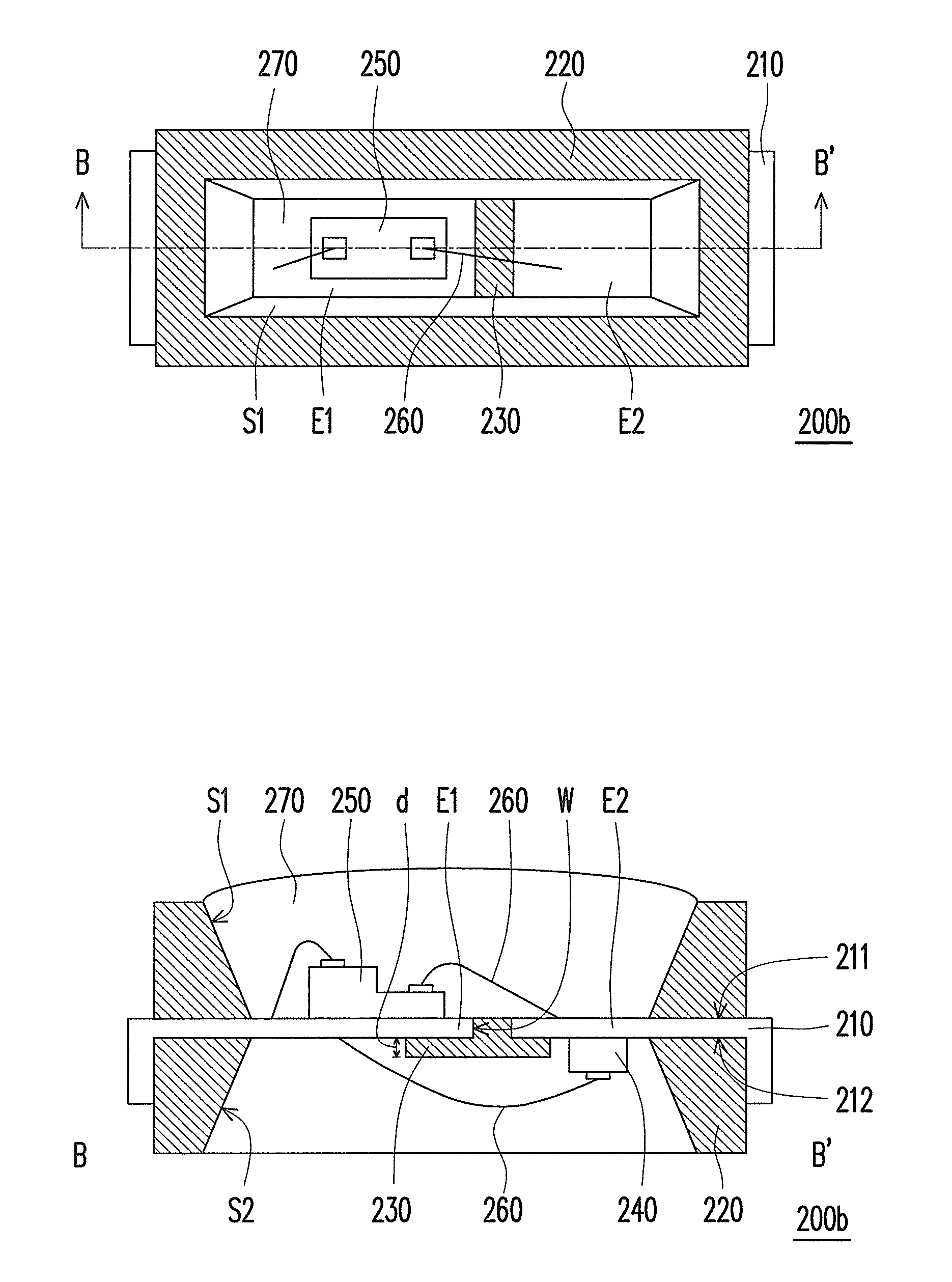
[0051]FIG. 2A is a schematic view of an LED package according to an embodiment of the present invention. FIG. 2B is a schematic cross-sectional view illustrating the LED package shown in FIG. 2A taken along line B-B′. Referring to FIG. 2A and FIG. 2B, the LED package 200a of the present embodiment includes a carrier 210, a package housing 220, a strength enhancement structure 230, an ESD protector 240, and an LED chip 250. The carrier 210 has a first surface 211 and a second surface 212 opposite to the first surface 211. The first surface 211 includes a first electrode E1 and a second electrode E2, wherein a gap W is between the first electrode E1 and the second electrode E2. The package housing 220 is disposed on the carrier 210 and has a first aperture S1 and a second aperture S2, wherein the first surface 211 is exposed by the first aperture S1 while the second surface 212 is exposed by the second aperture S2. The strength enhancement structure 230 is disposed on the carrier 210 ...


PUM


Abstract

A light emitting diode (LED) package is provided. The LED package includes a carrier, a package housing, a strength enhancement structure, an ESD protector and an LED chip. The carrier has a first surface and a second surface. The carrier includes a first electrode and a second electrode, wherein a gap is between the first electrode and the second electrode. The package housing is disposed on the carrier and has a first aperture and a second aperture. The first surface is exposed by the first aperture while the second surface is exposed by the second aperture. The strength enhancement structure is disposed at the gap. The ESD protector is disposed on the carrier and located within the second aperture. The LED chip is disposed on the carrier and located within the first aperture, wherein the ESD protector and the LED chip is electrically connected to the carrier.

Description

CROSS-REFERENCE TO RELATED APPLICATION[0001]This application is a continuation-in-part of and claims priority benefit of an application Ser. No. 11 / 535,991, filed on Sep. 28, 2006, which claims the priority benefit of Taiwan patent application serial no. 95106043, filed on Feb. 23, 2006. This application also claims he priority benefit of P.R.C. patent application serial no. 200810178897.1, filed on Dec. 8, 2009. The entirety of each of the above-mentioned patent application is hereby incorporated by reference herein and made a part of specification.BACKGROUND OF THE INVENTION[0002]1. Field of the Invention[0003]The present invention relates to a package and a fabricating method thereof. More particular, the present invention relates to a light emitting diode (LED) package with and a fabricating method thereof.[0004]2. Description of Related Art[0005]Due to advantages of long lifetime, small volume, great resistance to vibration, low heat emission, and low power consumption, LEDs ha...

Claims


Application Information

Patent Timeline
Patent Type & Authority Applications(United States)
IPC IPC(8): H01L33/00H01L21/50
CPCH01L25/167H01L2224/48091H01L2224/48247H01L2224/49107H01L2224/16245H01L2924/00014H01L2224/04042H01L2924/00011H01L2224/0401
Inventor LAI, KOU-RUEHYANG, GWO-SHIIHO, KUNG-CHITSAI, HU-CHENWANG, WEN-CHUAN
Owner NOVALITE OPTRONICS CORP
Why Eureka
Try Eureka