Circuit and Method for Clock Skew Compensation in Voltage Scaling

a clock skew and voltage scaling technology, applied in the field of circuits and methods for clock skew compensation in voltage scaling, can solve the problems of critical power consumption and power management, register may not function correctly, and the clock skew will typically increas

Inactive Publication Date: 2010-04-15
TAIWAN SEMICON MFG CO LTD
View PDF0 Cites 21 Cited by
  • Summary
  • Abstract
  • Description
  • Claims
  • Application Information

AI Technical Summary

Benefits of technology

[0007]These and other problems are generally solved or circumvented, and technical advantages are generally achieved, by embodiments of the present invention, which provides circuits and methods for automatically compensating for clock skew between portions of the circuitry, or power domains. The circuits a

Problems solved by technology

In integrated circuits, power consumption and management of power is a critical issue.
A problem that inherently arises when supply voltage level scaling is used in an integrated circuit is cross power domain clock skew.
That is, when a clock signal is used in two power domains, and one of them has a voltage supply that changes due to voltage scaling, an increase in clock skew will typically occur.
A

Method used


Image

  • Circuit and Method for Clock Skew Compensation in Voltage Scaling
  • Circuit and Method for Clock Skew Compensation in Voltage Scaling
  • Circuit and Method for Clock Skew Compensation in Voltage Scaling

Examples


Embodiment Construction

[0025]The making and using of the presently preferred embodiments are discussed in detail below. It should be appreciated, however, that the present invention provides many applicable inventive concepts that can be embodied in a wide variety of specific contexts. The specific embodiments discussed are merely illustrative of specific ways to make and use the invention, and do not limit the scope of the invention.

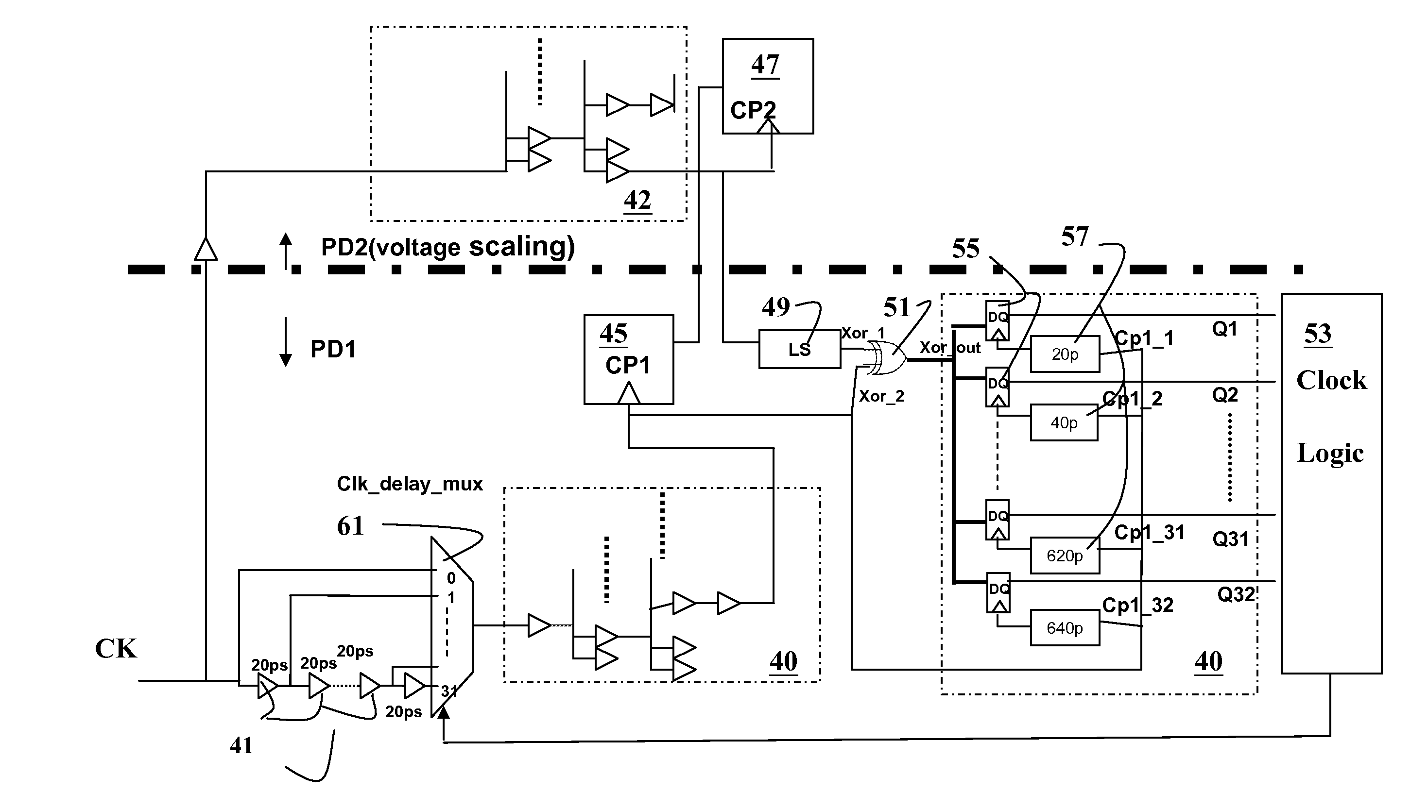
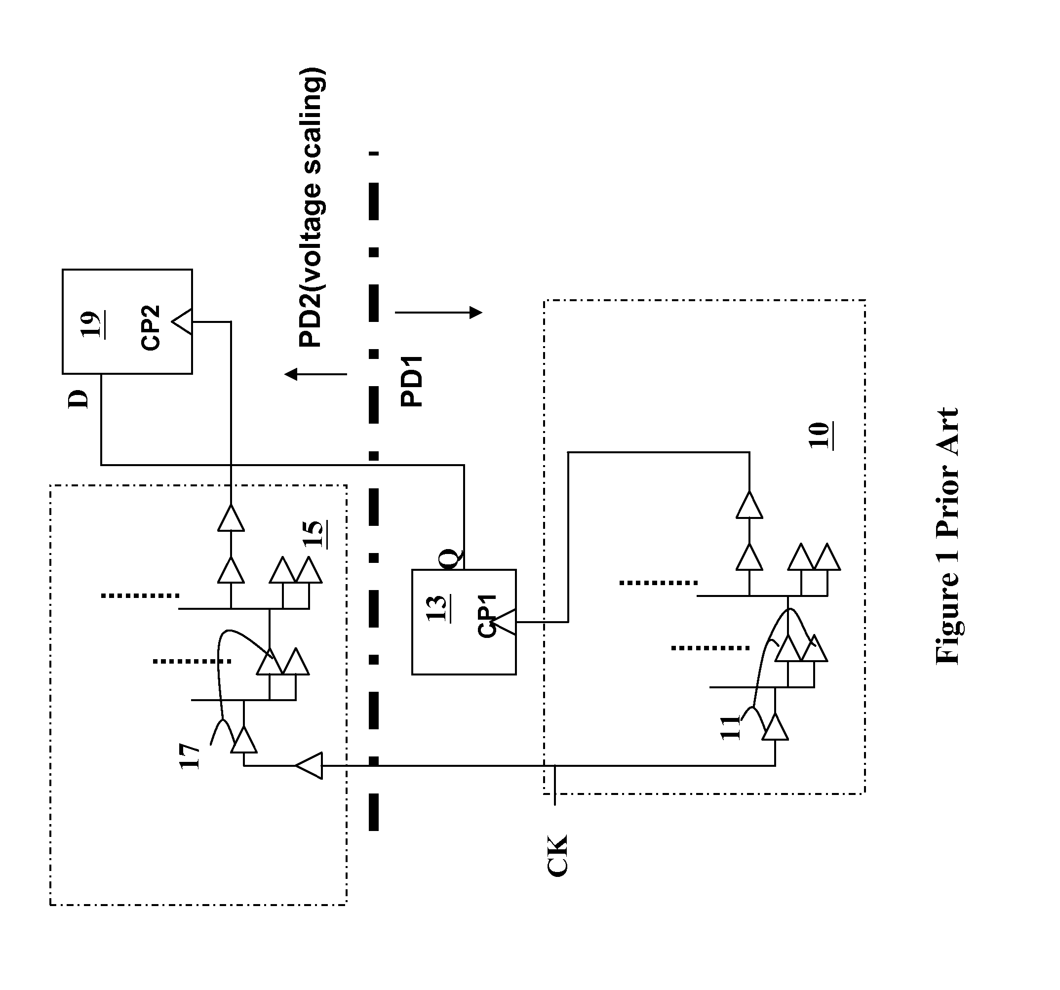
[0026]FIG. 4 depicts in a circuit diagram an illustrative exemplary embodiment of a voltage scaling clock skew compensation circuit of the present invention. In FIG. 4, a clocked circuit 47, for example a register, receives a clock pulse CP2 from a clock tree 42. The clock tree may be a single buffer but is more typically a plurality of buffers arranged to provide a more or less equal clock delay to the registers in power domain PD2. Circuit 47 and clock tree 42 are located in a power domain region PD2 of an integrated circuit, which is subject to voltage scaling. Another clo...


PUM


Abstract

Circuit and methods for automatic clock skew compensation in circuits having two power domains. When one of the power domains is operated with a lowered supply voltage, lowering the supply voltage tends to slow the clock pulse and produces clock skew. Circuitry is provided for selectively delaying the clock pulse in one of the power domains to reduce the clock skew by comparing the clock pulses, and then automatically delaying the clock pulse in one of the domains by a delay determined to minimize the skew. A method is provided where the clock skew between two clock pulses is determined and the delay needed in one of the clock pulses to reduce the skew is determined by sampling the clock skew using a plurality of delays at multiples of a minimum delay, and then automatically delaying the one clock pulse by selecting an appropriate delay. The method may be iterated.

Description

TECHNICAL FIELD[0001]The present invention relates to circuits and methods for providing improved clock skew compensation in semiconductor devices with voltage scaling. Voltage scaling is increasingly used to conserve power in integrated circuit devices by reducing the supply power (typically referred to as “Vdd”) to a portion of the circuitry during certain periods. The clock in use in the portion of the circuit subject to voltage scaling often crosses the power domains, so that the same clock timing is in use in another portion of the circuit that has different supply voltages. Reducing the supply voltage in one power domain or portion of the integrated circuit while maintaining the supply voltage in another domain or portion produces additional clock skew, which must be addressed. The present invention is directed to providing an improved circuit and methods that effectively provide efficient and effective clock skew compensation for integrated circuits using voltage scaling.BACK...

Claims


Application Information

Patent Timeline
IPC IPC(8): H03K5/12
CPCH03K19/00323G06F1/10
Inventor CHANGCHEIN, WEI-PINYING, SHU YIHSUEH, FU-LUNG
Owner TAIWAN SEMICON MFG CO LTD
Why Eureka
Try Eureka