
Semiconductor device having vertically aligned pillar structures that have flat side surfaces and method for manufacturing the same

a technology of pillar structure and side surface, which is applied in the direction of semiconductor device, basic electric element, electrical apparatus, etc., can solve the problems of voids being formed at the conductive layer of the gate, difficult and inability to completely fill the space between the pillar structure and the conductive layer

Active Publication Date: 2010-04-22
SK HYNIX INC
View PDF2 Cites 39 Cited by
  • Summary
  • Abstract
  • Description
  • Claims
  • Application Information

AI Technical Summary

Benefits of technology

[0010]Embodiments of the present invention are directed to a semiconductor device which can aid in stabilizing a process for forming a vertical transistor and a method for manufacturing the same.
[0011]Also, embodiments of the present invention are directed to a semiconductor device which can improve the performance characteristics and the reliability of the resultant semiconductor device and a method for manufacturing the same.

Problems solved by technology

Conventional techniques in fabricating vertical transistors also suffer from voids being formed at conductive layers for the gate.
That is it is difficult to completely fill in the spaces between the pillar structures with the conductive layers because of the presence of the neck parts.
As a result, of conventionally forming a conductive layer for gates, voids can be produced in these spaces.
Furthermore, when subsequently etching these conductive layers for gates, adjacent portions of the semiconductor substrate for gates are prone to being lost.
As a result fabricating the vertical transistors with conventional techniques, the performance characteristics of the resultant semiconductor devices are likely to be degraded.

Method used


Image

  • Semiconductor device having vertically aligned pillar structures that have flat side surfaces and method for manufacturing the same
  • Semiconductor device having vertically aligned pillar structures that have flat side surfaces and method for manufacturing the same
  • Semiconductor device having vertically aligned pillar structures that have flat side surfaces and method for manufacturing the same

Examples


first embodiment

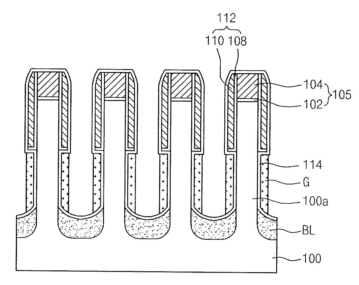
[0031]FIG. 1 is a sectional view illustrating a semiconductor device in accordance with the present invention.

[0032]Referring to FIG. 1, pillar structures 100a having hard masks 105 are formed on a semiconductor substrate 100. For example, the hard masks 105 have the stack structure of an oxide layer 102 and a nitride layer 104. The pillar structures 100a according to the embodiment of the present invention have substantially flat side surfaces. Spacers 112 are formed on the upper portions of the pillar structures 100a, and gates G are formed on the lower portions of the pillar structures 100a in such a way as to surround the sidewalls of the pillar structures 100a under the spacers 112. The spacers 112 include an oxide layer 108 and a nitride layer 110.

[0033]Therefore, the semiconductor device in accordance with the first embodiment of the present invention has the pillar structures having substantially flat side surfaces instead of the conventional pillar structures that have tape...

second embodiment

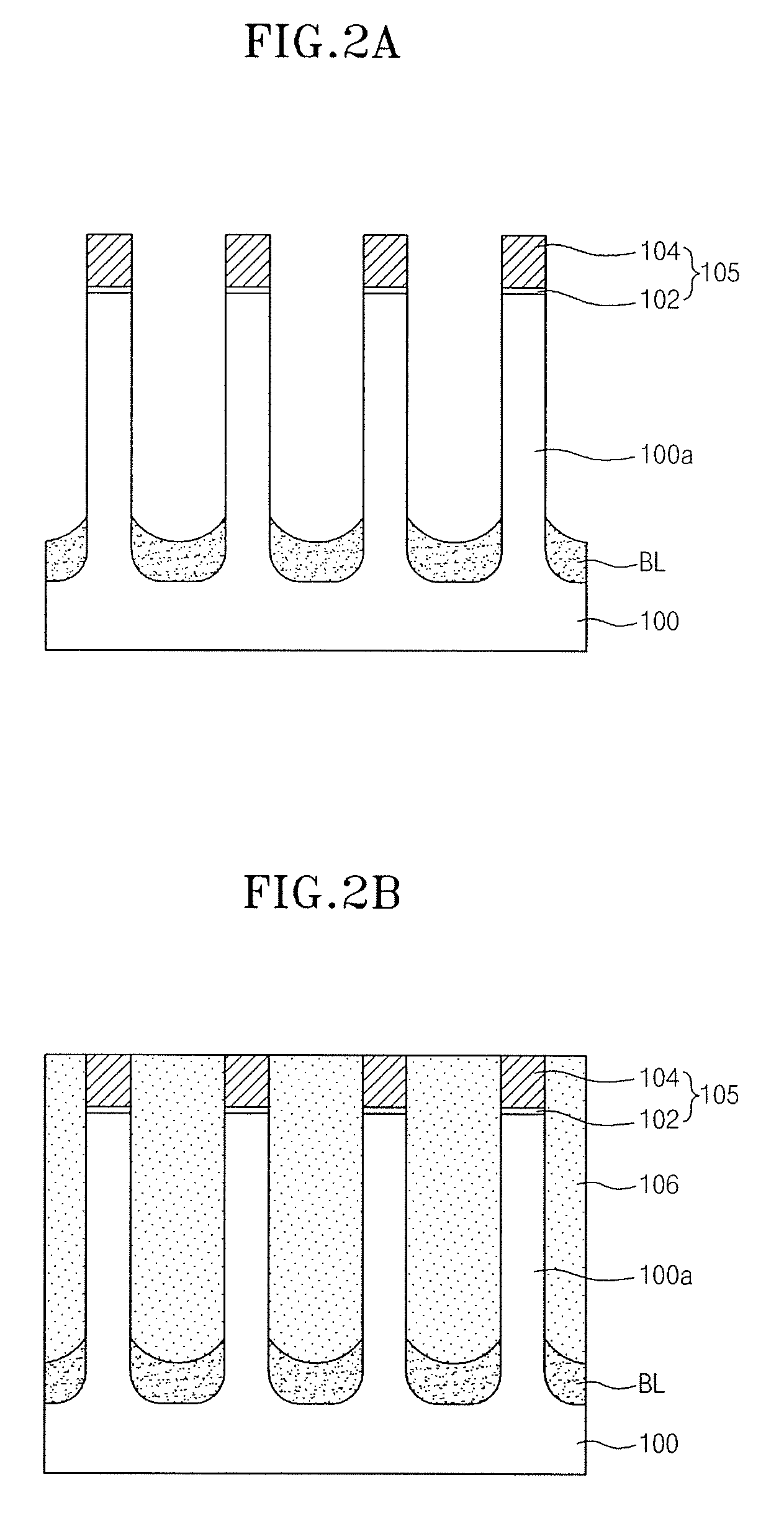
[0036]FIGS. 2A through 2L are sectional views illustrating the processes of a method for manufacturing a semiconductor device in accordance with the present invention. The method will be described below.

[0037]Referring now to FIG. 2A, an oxide layer 102 and a nitride layer 104 are shown sequentially formed on a semiconductor substrate 100. The nitride layer 104 preferably has a thickness of about 500˜1,000 Å which is less than about 1,500 Å as compared to the conventional arts. The hard masks 105 is are formed by selectively etching the nitride layer 104 and the oxide layer 102 which exposes portions of the semiconductor substrate 100.

[0038]Pillar structures 100a having substantially flat side to surfaces are next formed by anisotropically etching into exposed portions of the semiconductor substrate 100 which uses the hard masks 105 as etch mask barriers. The pillar structures 100a are preferably formed to have a height of, for example, 1,000˜3,000 Å. Preferably, the pillar structur...


PUM


Abstract

A semiconductor device having vertically aligned transistors made from pillar structures that have flat side surfaces is presented. The semiconductor device includes a semiconductor substrate, spacers, and gates. The semiconductor substrate has lo pillar structures that have flat side surfaces. The spacers are on sidewalls only on the upper portions of the pillar structures. The gates surround lower portions of the pillar structures.

Description

CROSS-REFERENCE TO RELATED APPLICATIONS[0001]The present application claims priority to Korean patent application number 10-2008-0103741 filed on Oct. 22, 2008, which is incorporated herein by reference in its entirety.BACKGROUND OF THE INVENTION[0002]The present invention relates to a semiconductor device and a method for manufacturing the same, and more particularly, to a semiconductor device that can stabilize a process for forming a vertical transistor, thereby improving the characteristics and the reliability of a semiconductor device, and a method for manufacturing the same.[0003]As the integration level of a semiconductor device increases, the area that is occupied by each unit cell decreases when viewed from above. Corresponding to the need to decrease in the area of the unit cell, various alternate methods for forming transistors, bit lines and capacitors within these diminished areas have been researched. In one approach, a semiconductor device having the structure of a tr...

Claims


Application Information

Patent Timeline
Patent Type & Authority Applications(United States)
IPC IPC(8): H01L29/78H01L21/8234
CPCH01L29/66666H01L21/823487
Inventor SHIN, JONG HANPARK, HYUNG SOONPARK, JUM YONGKIM, SUNG JUNLEE, YOUNG JU
Owner SK HYNIX INC
Features
  • Generate Ideas
  • Intellectual Property
  • Life Sciences
  • Materials
  • Tech Scout
  • Unparalleled Data Quality
  • Higher Quality Content
  • 60% Fewer Hallucinations
Learn More