MEMS package and packaging method thereof

a micro electromechanical system and micro-electromagnetic system technology, applied in the direction of fluid pressure measurement, acceleration measurement using interia forces, instruments, etc., can solve the problems of reducing yield, wafer level packages may not be manufactured, and different electrical characteristics between designed and manufactured mems devices, so as to reduce the snr of the mems device, improve yield, and reduce the effect of parasitic resistance and parasitic capacitan

Inactive Publication Date: 2010-04-22
ELECTRONICS & TELECOMM RES INST
View PDF15 Cites 42 Cited by
  • Summary
  • Abstract
  • Description
  • Claims
  • Application Information

AI Technical Summary

Benefits of technology

[0010]An MEMS device of the present invention can be directly bonded to an MEMS driving electronic device to improve yield. Also, an MEMS package can be manufactured on a wafer or chip level. In addition, effects of a parasitic resistance and a parasitic capacitance can be reduced to reduce the SNR of the MEMS device. Moreover, the MEMS device can be packaged and then bonded to the MEMS driving electronic device so as to realize a dual package structure. Thus, time and cost required for packaging can be saved to improve productivity.

Problems solved by technology

However, in the first method, a difference in electrical characteristics occurs between a designed MEMS device and a manufactured MEMS device due to a parasitic resistance, a parasitic capacitance, etc. caused by the wire bonding.
Thus, a chip level package may be manufactured, but a wafer level package may not be manufactured.
However, in the third method, yield may be more reduced than when the MEMS device and the MEMS driving electronic device are manufactured on different wafers, due to yield variables of the MEMS device and the MEMS driving electronic device.
In other words, the third method requires large amounts of cost and time to mass-produce MEMS chips and MEMS driving electronic devices.

Method used


Image

  • MEMS package and packaging method thereof
  • MEMS package and packaging method thereof
  • MEMS package and packaging method thereof

Examples


Embodiment Construction

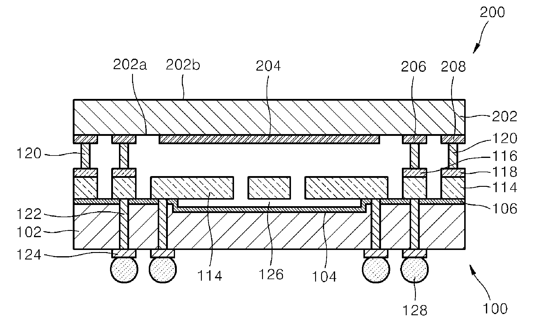
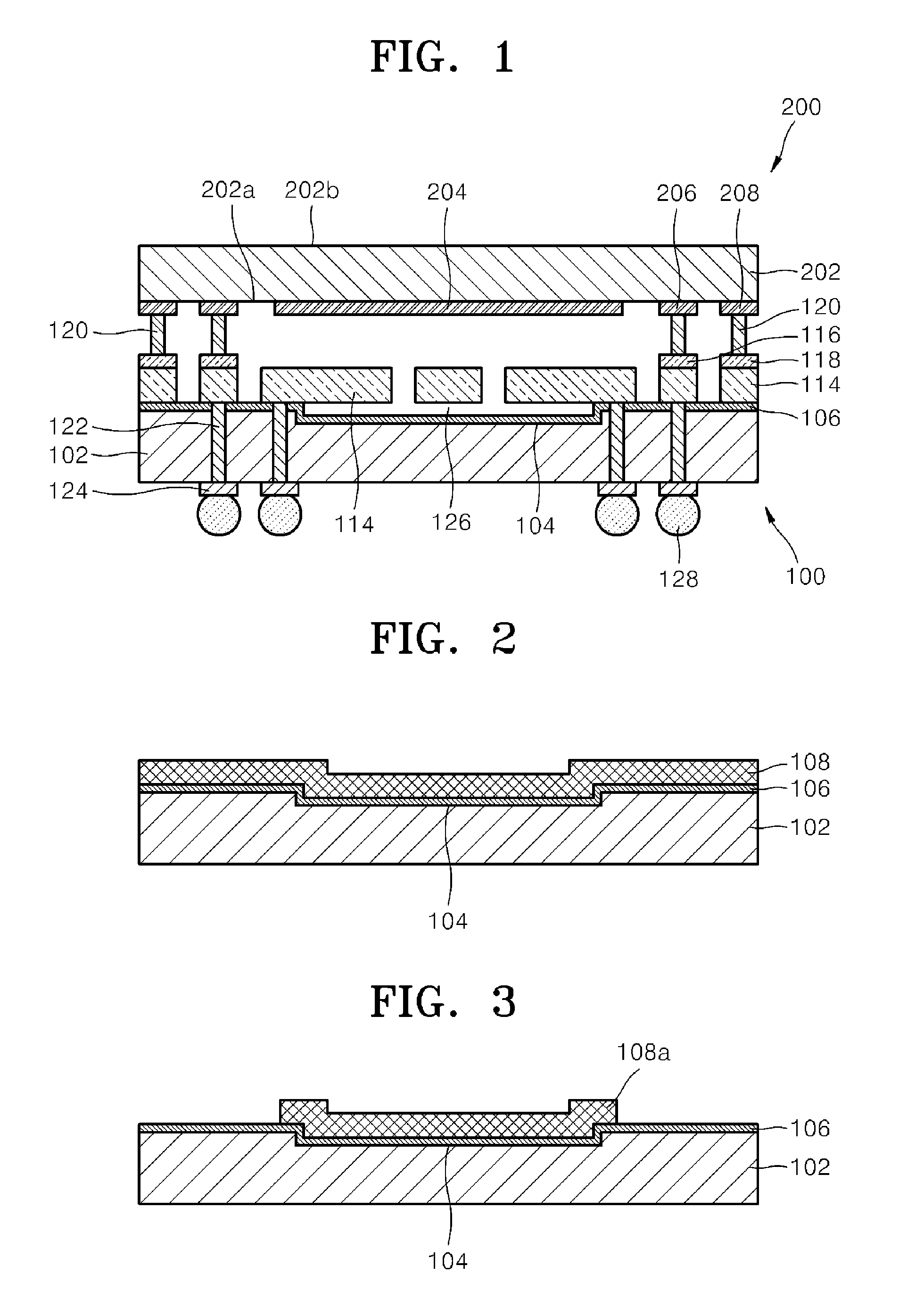
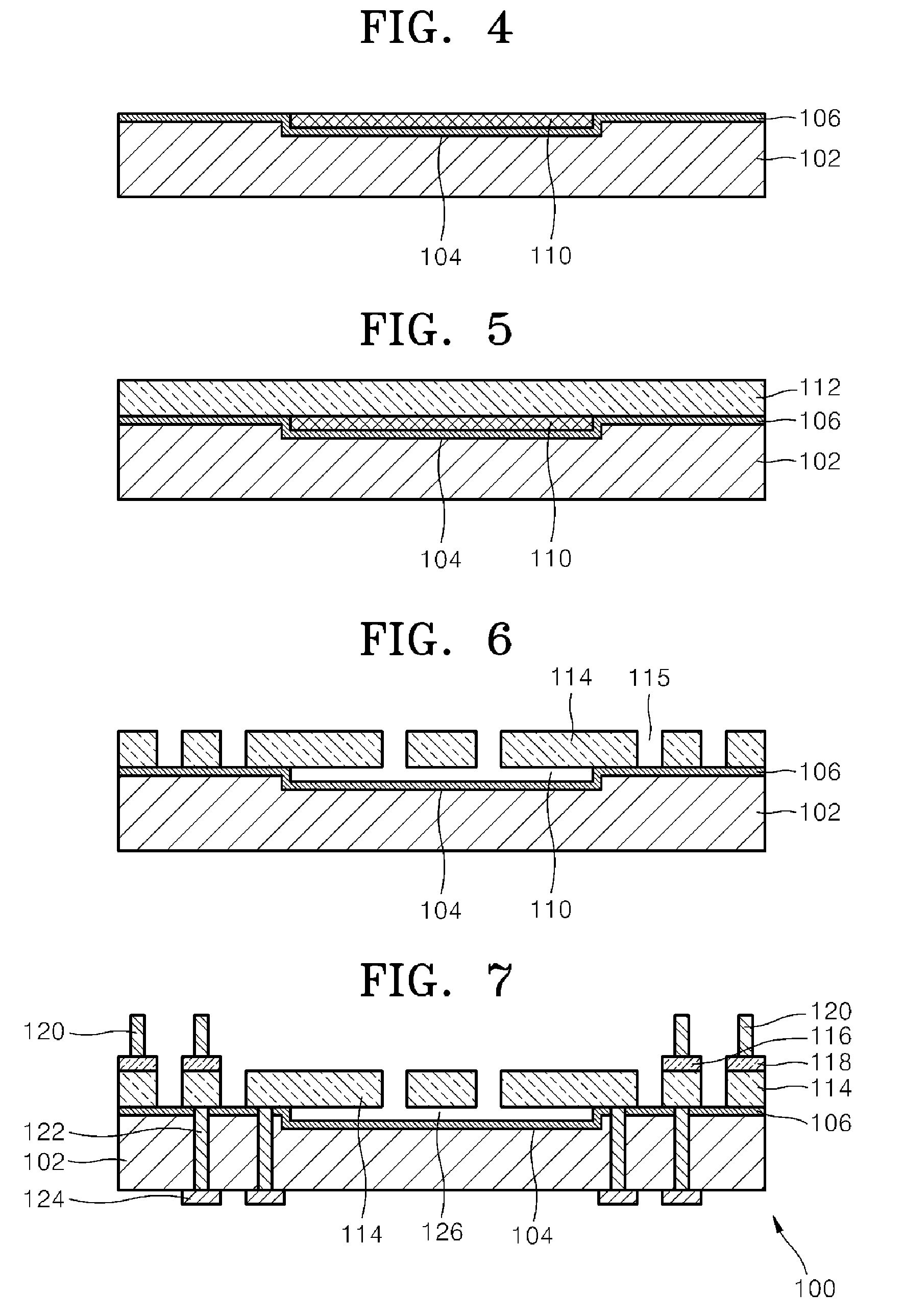
[0018]Hereinafter, the present invention will now be described more fully with reference to the accompanying drawings, in which exemplary embodiments of the invention are shown. The invention may, however, be embodied in many different forms and should not be construed as being limited to the embodiments set forth herein; rather, these embodiments are provided so that this disclosure will be thorough and complete, and will fully convey the concept of the invention to those skilled in the art. In the drawings, the thicknesses of layers and regions are exaggerated for clarity.

[0019]In the present invention a Micro Electro-Mechanical System (MEMS) device and an MEMS driving electronic device are directly bonded to each other to face each other so as to package an MEMS package. Furthermore, various methods may be used to package the MEMS package, and an order of packaging the MEMS package is not limited but may be varied. Embodiments of the present invention will now be described with r...


PUM


Abstract

Provided are a Micro Electro-Mechanical System (MEMS) package and a method of packaging the MEMS package. The MEMS package includes: a MEMS device including MEMS structures formed on a substrate, first pad electrodes driving the MEMS structures, first sealing parts formed at an edge of the substrate, and connectors formed on the first pad electrodes and the first sealing parts; and a MEMS driving electronic device including second pad electrodes and second sealing parts respectively corresponding to the first pad electrodes and the first sealing parts to be sealed with and bonded to the MEMS device through the connectors to form an air gap having a predetermined width.

Description

TECHNICAL FIELD[0001]The present invention relates to a Micro Electro-Mechanical System (MEMS) package and a packaging method thereof, and more particularly, to a package of an MEMS device and an electronic device for driving the MEMS device and a packaging method thereof.BACKGROUND ART[0002]The methods of connecting a Micro Electro-Mechanical system (MEMS) device to an electronic device for driving the MEMS device (a driving circuit device), e.g., an application specific integrated circuit (ASIC) chip, can be classified into three types.[0003]In a first method, an upper, lower, or side portion of a packaged MEMS device is connected to an MEMS driving electronic device using Au wire bonding. In a second method, the packaged MEMS device is bonded to the MEMS driving electronic device using flip-chip bonding. In a third method, the MEMS device and the MEMS driving electronic device are manufactured on a wafer and then connected to each other using electrodes.[0004]However, in the firs...

Claims


Application Information

Patent Timeline
Patent Type & Authority Applications(United States)
IPC IPC(8): H01L29/84H01L21/02
CPCB81C1/0023B81C2203/0118B81B2207/096B81B2207/012H01L2224/13H01L29/00
Inventor JUNG, SUNG-HAE
Owner ELECTRONICS & TELECOMM RES INST
Why Eureka
Try Eureka