Contactor and method of production of contactor

a technology of contactor and contactor plate, which is applied in the field of contactor, can solve the problems of plastic deformation, change of state between the ic device and the contactor, and inability to perform accurate tests in some cases, and achieve good test precision

Inactive Publication Date: 2010-04-29
ADVANTEST CORP
View PDF15 Cites 20 Cited by
  • Summary
  • Abstract
  • Description
  • Claims
  • Application Information

AI Technical Summary

Benefits of technology

[0010]An object of the present invention is to provide a contactor enabling heights of front end parts to be maintained over a long period of time and a good test precision to be secured.

Problems solved by technology

However, nickel-cobalt is a metal material, so repeated contact with input / output terminals of an IC device results in plastic deformation.
For this reason, along with repeated tests, the contact state between the IC device and the contactor changes and it is impossible to perform accurate tests in some cases.
Further, the nickel-cobalt layers expand due to heat by the effects of the thermal stress applied to the IC device at the time of testing, so the difference in heat expansion from the silicon composing the beam parts causes warping in the silicon finger contactor and deviation in the height of the front end parts contacting the IC device with respect to the IC device in some cases.

Method used


Image

  • Contactor and method of production of contactor
  • Contactor and method of production of contactor
  • Contactor and method of production of contactor

Examples


Embodiment Construction

[0135]Below, an embodiment of the present invention will be explained based on the drawings.

[0136]FIG. 1 is a schematic view showing a test apparatus in an embodiment of the present invention, while FIG. 2 is a conceptual view showing the connection relationship between a test head and a probe card used in the test apparatus of FIG. 1.

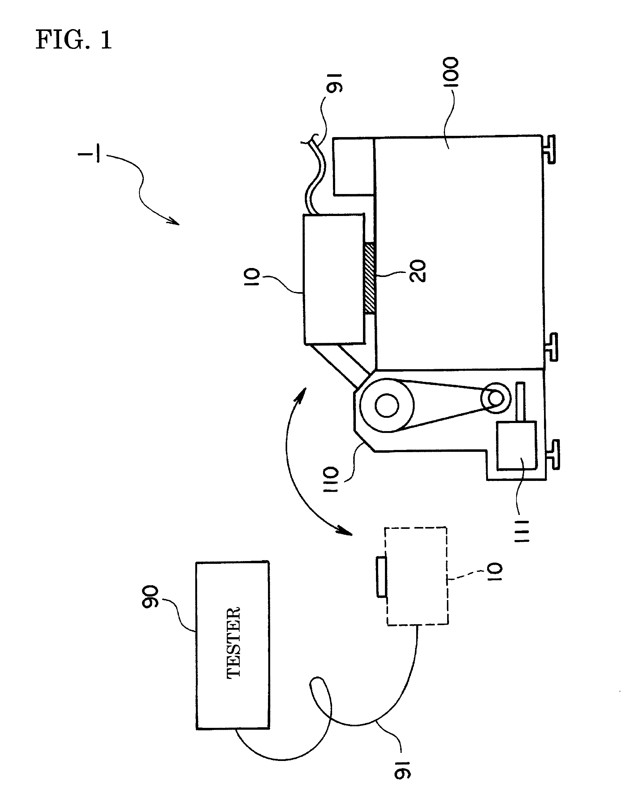
[0137]The test apparatus 1 according to the present embodiment, as shown in FIG. 1, comprises a test head 10, a tester 90 (test apparatus body), and a prober 100. The tester 90 is electrically connected through a cable bundle 91 to the test head 10 and can input and output DC signals or digital signals to and from an IC device built in a silicon wafer (hereinafter also referred to as a “wafer under test”) 200. The test head 10 is arranged on a prober 100 by a manipulator 110 and drive motor 111.

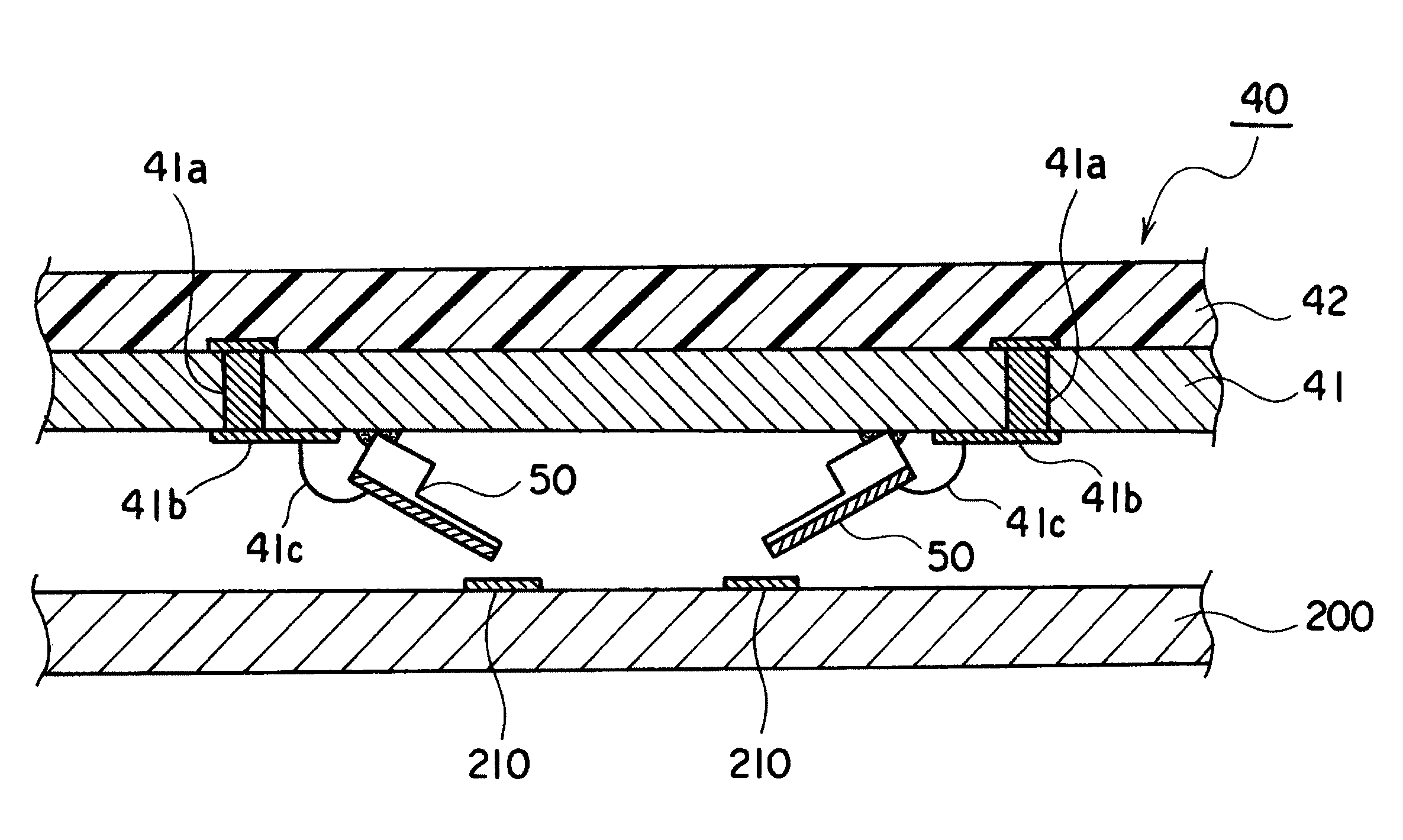
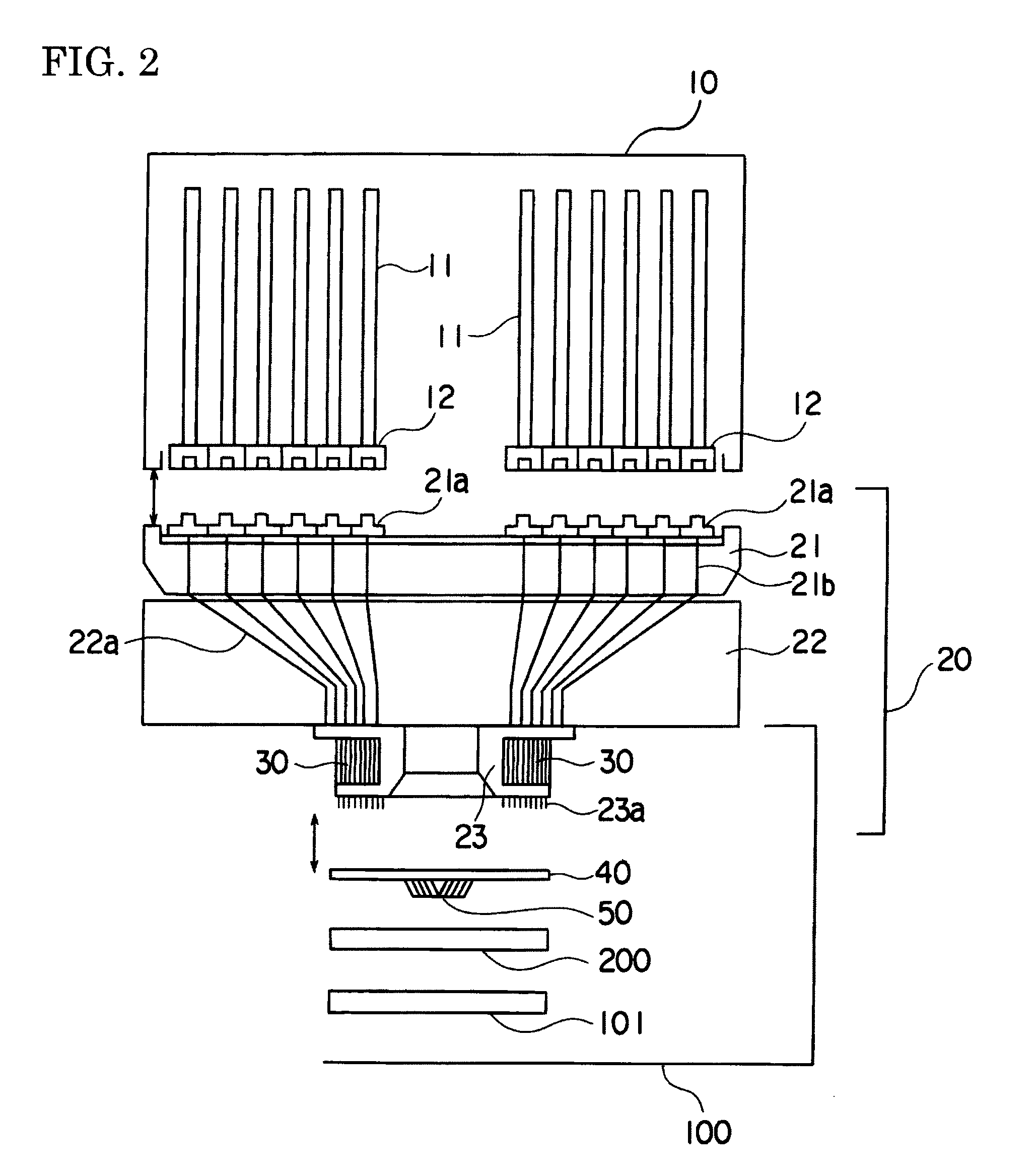
[0138]As shown in FIG. 1 and FIG. 2, a large number of printed circuit boards 11 are provided inside the test head 10. These printed circuit boards 11 are conne...


PUM

PropertyMeasurementUnit
thicknessaaaaaaaaaa
resistivityaaaaaaaaaa
thicknessaaaaaaaaaa

Abstract

A contactor includes: a silicon layer composing a part of beam part with a rear end side provided at a base part and with a front end side sticking out from the base part; SiO2 layer as an insulating layer formed on the silicon layer; and a conductive layer formed on the SiO2 layer.

Description

TECHNICAL FIELD[0001]The present invention relates to a contactor for contacting pads, electrodes, leads, or other input / output terminals provided at an integrated circuit or other electrical circuit formed on a semiconductor wafer, semiconductor chip, printed circuit board, etc. (hereinafter also referred to representatively as an “IC device”) and establishing an electrical connection with the IC device when testing an IC device and a method of production of such a contactor.BACKGROUND ART[0002]A large number of semiconductor integrated circuit devices are built in a silicon wafer etc., then are diced, bonded, packaged, and otherwise processed to form finished electronic devices. These IC devices are subjected to operational tests before shipment. These IC tests are run in the state of the finished products and in the state of the wafer.[0003]When testing an IC device in the wafer state, probe needles (hereinafter also referred to as “contactors”) provided on a probe card of the el...

Claims


Application Information

Patent Timeline
Patent Type & Authority Applications(United States)
IPC IPC(8): H01R13/02H01R13/03G01R31/02H01R43/16
CPCG01R1/06727G01R1/06761Y10T29/49204G01R3/00G01R1/07342G01R1/073
Inventor KITAZUME, HIDENORIASANO, KOJI
Owner ADVANTEST CORP
Why Eureka
Try Eureka