Liquid crystal display device and method for fabricating the same

a technology of liquid crystal display and liquid crystal, which is applied in the direction of non-linear optics, instruments, optics, etc., can solve the problems of large process time and expense burden, inability to rapidly recover the substrate from a shifted state to an original state, and inability to observe luminous defects, etc., to achieve the effect of reducing the amount of liquid crystals filled

Inactive Publication Date: 2010-04-29
LG DISPLAY CO LTD
View PDF5 Cites 28 Cited by
  • Summary
  • Abstract
  • Description
  • Claims
  • Application Information

AI Technical Summary

Benefits of technology

[0014]An object of the present invention is to provide a liquid crystal display device which maintains a desired vertical gap between opposite substrates, prevents a substrate shift phenomenon from occurring between the substrates when the substrates are subjected to a touch, or prevent generation of display defects caused by application of a pressure, and reduces the amount of liquid crystal material used, and a method for fabricating the liquid crystal display device.
[0016]To achieve these objects and other advantages and in accordance with the purpose of the invention, as embodied and broadly described herein, a liquid crystal display device comprises first and second substrates facing each other; gate lines and data lines formed on the first substrate such that the gate lines and the data lines intersect each other to define pixel regions; thin film transistors formed at respective intersections of the gate lines and the data lines; a black matrix layer formed on the second substrate such that the black matrix layer corresponds to a region other than the pixel regions; color filter layers extending in an extension direction of the data lines in respective pixel regions; a liquid crystal layer interposed between the first and second substrates; first column spacers formed on one of the first and second substrates such that each first column spacer corresponds to an associated one of the gate lines or to a channel region of an associated one of the thin film transistors to maintain a cell gap between the first and second substrate; and spacer patterns formed on one of the first and second substrates such that each spacer pattern corresponds to at least one of an associated one of the gate lines and an associated one of the data lines, thereby forming a first gap between the spacer pattern and the other substrate facing the spacer pattern, and reducing an amount of liquid crystals filled between the first and second substrates.
[0017]In another aspect of the present invention, a method for fabricating a liquid crystal display device, comprising: forming gate lines and data lines on a first substrate such that the gate lines and the data lines intersect each other to define pixel regions, and forming thin film transistors at respective intersections of the gate lines and the data lines; forming a black matrix layer on the second substrate such that the black matrix layer corresponds to a region other than the pixel regions; forming color filter layers on a second substrate such that the color filter layers extend in an extension direction of the data lines in respective pixel regions; forming first column spacers on one of the first and second substrates such that each first column spacer corresponds to an associated one of the gate lines or to a channel region of an associated one of the thin film transistors while maintaining a cell gap between the first and second substrate; forming spacer patterns on one of the first and second substrates such that each spacer pattern corresponds to at least one of an associated one of the gate lines and an associated one of the data lines, thereby forming a first gap between the spacer pattern and the other substrate facing the spacer pattern, and reducing an amount of liquid crystals filled between the first and second substrates; and bonding the first and second substrates such that a liquid crystal layer is formed between the first and second substrates.

Problems solved by technology

For this reason, there is a problem in a touch operation for a test, in which the surface of one of the first and second substrates is rubbed in a certain direction.
That is, there may be defects caused by the touch operation in that the substrate cannot be rapidly recovered from a shifted state to an original state, or a depression stain such as a trace is formed in a region where a pressure is locally applied to the substrate.
Thus, various luminous defects may be observed after the touch operation.
In addition, although liquid crystals are filled in a space between the first and second substrates, the filling of the liquid crystals causes a large burden in terms of process time and expense.
In association with the manufacture of panels, in particular, efforts to reduce the use amount of liquid crystal materials have been made because the use of liquid crystals causes a large burden in terms of process time and expense.
Furthermore, with an LCD device including column spacers configured to simply maintain a desired vertical gap between the first and second substrates, display defects may be generated in a test involving a touch operation, in which the surfaces of the substrates are rubbed, or local application of a pressure to the substrates.

Method used


Image

  • Liquid crystal display device and method for fabricating the same
  • Liquid crystal display device and method for fabricating the same
  • Liquid crystal display device and method for fabricating the same

Examples


Embodiment Construction

[0052]Reference will now be made in detail to the preferred embodiments of the present invention, examples of which are illustrated in the accompanying drawings. Wherever possible, the same reference numbers will be used throughout the drawings to refer to the same or like parts.

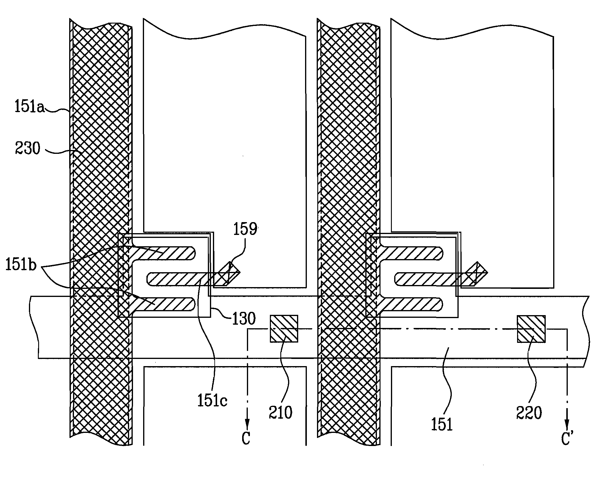
[0053]FIG. 4 is a plan view illustrating one pixel of an exemplary liquid crystal display (LCD) device according to the present invention, and column spacers and spacer patterns formed to correspond to the pixel. FIG. 5 is a cross-sectional view taken along lines II-II′, III-III′, and IV-IV′ of FIG. 4. As shown in FIGS. 4 and 5, each pixel of the LCD device according to the present invention includes R, G, and B sub-pixels. Each sub-pixel includes a gate line (“151” in FIG. 6) and a data line (“155a” in FIG. 6) intersecting each other. The gate line is shown extended in a horizontal direction. In each sub pixel, the data line is obtusely bent with respect to the gate line at a region, where the sub pixel is ...


PUM

PropertyMeasurementUnit
heightaaaaaaaaaa
heightaaaaaaaaaa
heightaaaaaaaaaa

Abstract

A liquid crystal display device includes first and second substrates facing each other; gate lines and data lines formed on the first substrate such that the gate lines and the data lines intersect each other to define pixel regions; thin film transistors formed at respective intersections of the gate lines and the data lines; a black matrix layer formed on the second substrate such that the black matrix layer corresponds to a region other than the pixel regions; color filter layers extending in an extension direction of the data lines in respective pixel regions; a liquid crystal layer interposed between the first and second substrates; first column spacers formed on one of the first and second substrates such that each first column spacer corresponds to an associated one of the gate lines or to a channel region of an associated one of the thin film transistors to maintain a cell gap between the first and second substrate; and spacer patterns formed on one of the first and second substrates such that each spacer pattern corresponds to at least one of an associated one of the gate lines and an associated one of the data lines, thereby forming a first gap between the spacer pattern and the other substrate facing the spacer pattern, and reducing an amount of liquid crystals filled between the first and second substrates.

Description

[0001]This is a continuation application of copending application Ser. No. 12 / 003,586, filed on Dec. 28, 2007, which is hereby incorporated by reference. This application claims the benefit of the Korean Patent Application No. 10-2007-070253, filed on Jul. 12, 2007, and Korean Patent Application No. 10-2007-098684, filed on Oct. 1, 2007, both of which are hereby incorporated by reference as if fully set forth herein.BACKGROUND OF THE INVENTION[0002]1. Field of the Invention[0003]The present invention relates to a liquid crystal display device, and more particularly, to a liquid crystal display device and a method for fabricating the same, which reduces the amount of liquid crystal material used in the liquid crystal display device in accordance with a particular column spacer formation process.[0004]2. Background of the Related Art[0005]With the progress of an information-dependent society, the demand for various display devices has increased. To meet such demands, efforts have rece...

Claims


Application Information

Patent Timeline
Patent Type & Authority Applications(United States)
IPC IPC(8): G02F1/1339G02F1/13
CPCG02F1/133371G02F1/136286G02F1/134363G02F1/13394
Inventor CHOI, YOUNG SEOKJUNG, YU HOLEE, SANG YONG
Owner LG DISPLAY CO LTD
Why Eureka
Try Eureka