Techniques for Use of Nanotechnology in Photovoltaics

Inactive Publication Date: 2010-05-06
GLOBALFOUNDRIES INC
View PDF19 Cites 13 Cited by
  • Summary
  • Abstract
  • Description
  • Claims
  • Application Information

AI Technical Summary

Problems solved by technology

Photovoltaic devices, such as photocells, are an important energy source that has thus far remained underutilized for widespread energy production due to undesirable efficiency and/or production cost factors.
Crystalline semic

Method used


Image

  • Techniques for Use of Nanotechnology in Photovoltaics
  • Techniques for Use of Nanotechnology in Photovoltaics
  • Techniques for Use of Nanotechnology in Photovoltaics

Examples


Embodiment Construction

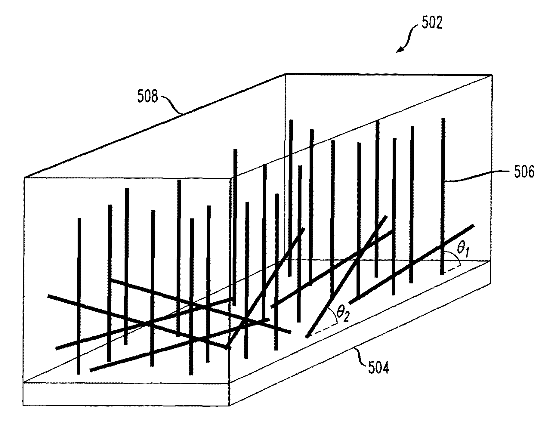
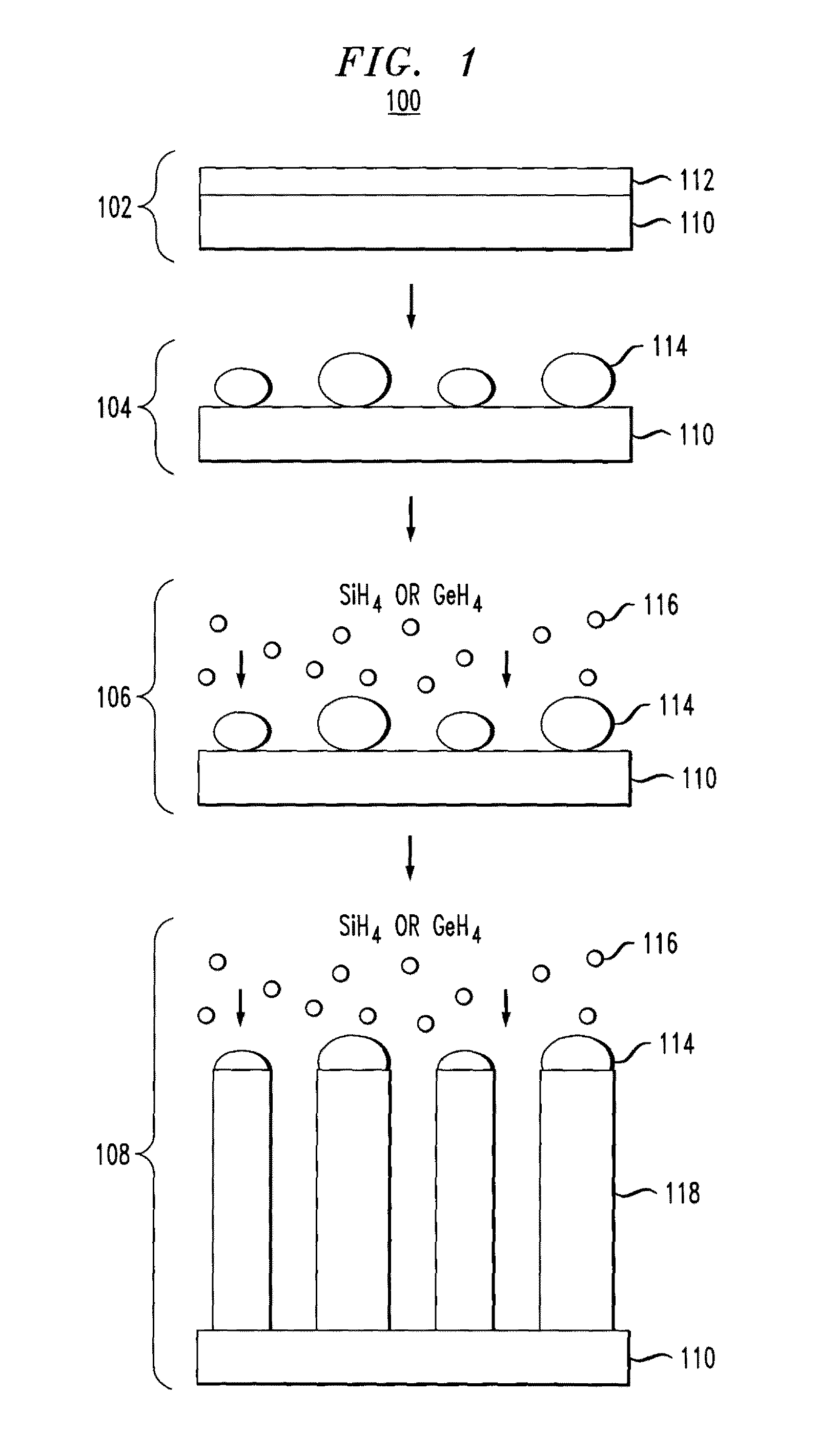
[0017]FIG. 1 is a diagram illustrating exemplary methodology 100 for growing a nanowire forest. The term “nanowire forest,” as used herein, refers to a plurality of nanowires attached to a substrate. As will be described in detail below, the growth of the nanowire forest is conducted in a chemical vapor environment.

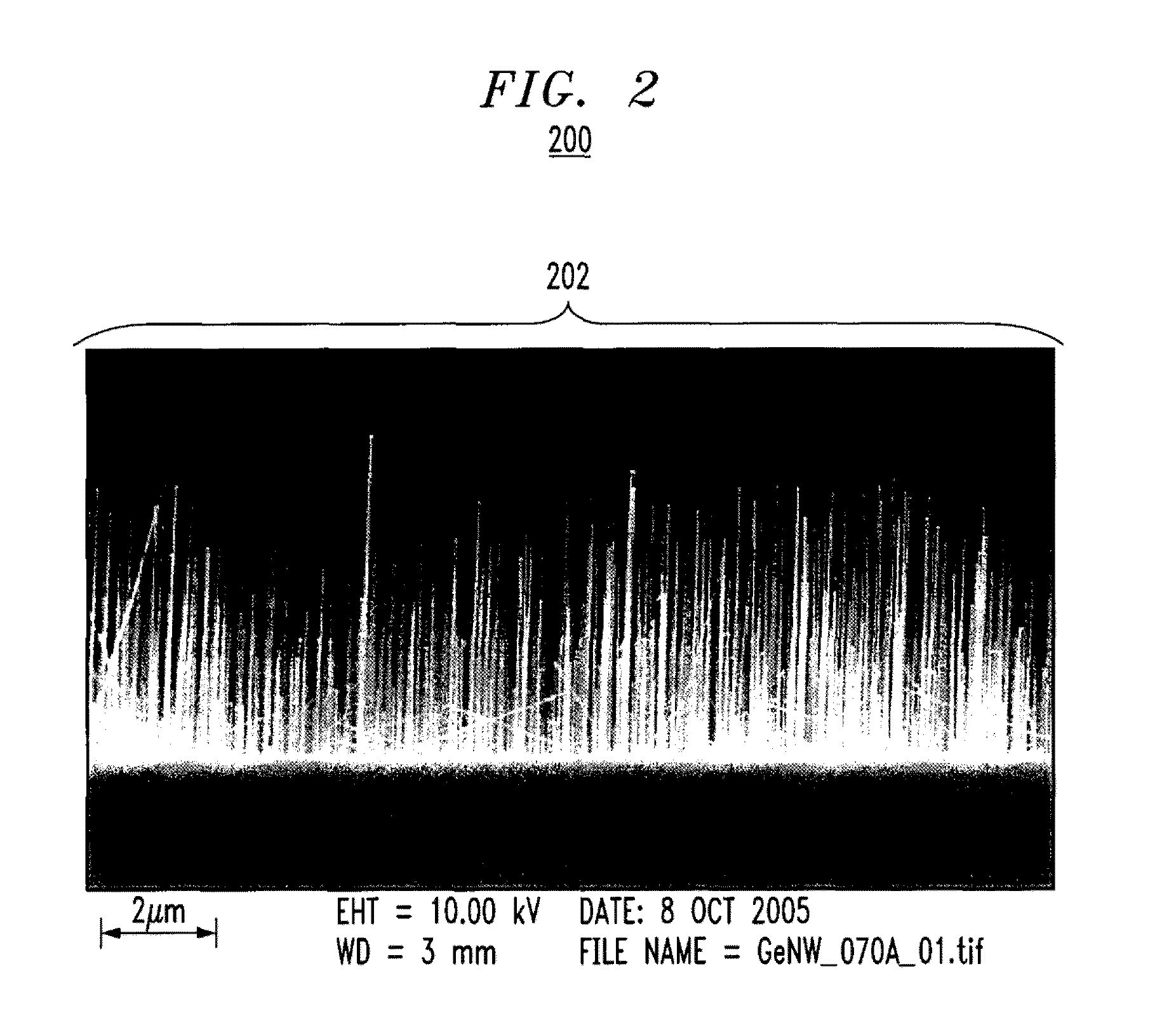
[0018]Nanowires are highly-anisotropic, rod-like crystals with diameters d of between about ten nanometers (nm) and about 70 nm and lengths L of between about 0.1 micrometers (μm) and about 100 μm. Due to the nanowires having large L to d ratios, the surface area of the substrate is increased by a factor (4L / d)f, wherein f denotes the fraction of the substrate area covered by nanowires. By way of example only, for a five percent substrate areal coverage, nanowires of diameter d=40 nm and length L=five μm will provide a surface area that is 25 times greater than that of the substrate alone.

[0019]While the present description is directed to nanowires being a preferred nanos...


PUM


Abstract

Techniques for combining nanotechnology with photovoltaics are provided. In one aspect, a method of forming a photovoltaic device is provided comprising the following steps. A plurality of nanowires are formed on a substrate, wherein the plurality of nanowires attached to the substrate comprises a nanowire forest. In the presence of a first doping agent and a first volatile precursor, a first doped semiconductor layer is conformally deposited over the nanowire forest. In the presence of a second doping agent and a second volatile precursor, a second doped semiconductor layer is conformally deposited over the first doped layer. The first doping agent comprises one of an n-type doping agent and a p-type doping agent and the second doping agent comprises a different one of the n-type doping agent and the p-type doping agent from the first doping agent. A transparent electrode layer is deposited over the second doped semiconductor layer.

Description

CROSS-REFERENCE TO RELATED APPLICATION(S)[0001]This application is a divisional of U.S. application Ser. No. 11 / 494,195 filed on Jul. 27, 2006 the disclosure of which is incorporated by reference herein.STATEMENT OF GOVERNMENT RIGHTS[0002]This invention was made with Government support under N66001-05-C-8043 awarded by Defense Advanced Research Projects Agency (DARPA). The Government has certain rights in this invention.FIELD OF THE INVENTION[0003]The present invention relates to use of nanotechnology in photovoltaics, and more particularly, to nanostructure-based photovoltaic devices.BACKGROUND OF THE INVENTION[0004]Photovoltaic devices, such as photocells, are an important energy source that has thus far remained underutilized for widespread energy production due to undesirable efficiency and / or production cost factors. For example, conventional photocells comprise a silicon-based substrate that includes a large-area p-n junction. Crystalline semiconductor substrates, such as sili...

Claims


Application Information

Patent Timeline
IPC IPC(8): H01L31/0352
CPCH01L31/035227H01L31/03529H01L31/068H01L31/1804H01L31/1808H01L31/1812Y10S977/936Y10S977/938Y10S977/813Y10S977/827Y10S977/743Y02E10/547Y02P70/521Y02P70/50
Inventor GUHA, SUPRATIKHAMANN, HENDRIK F.TUTUC, EMANUEL
Owner GLOBALFOUNDRIES INC
Why Eureka
Try Eureka