Surface acoustic wave element, surface acoustic wave device and methods for manufacturing the same

a surface acoustic wave and element technology, applied in the direction of filters, generators/motors, instruments, etc., can solve the problems of undesirable leakage current flowing through the sample, and the inability of the saw sensor to accurately sense the target material, so as to achieve the effect of preventing the flow of leakage curren

Inactive Publication Date: 2010-05-06
SAMSUNG ELECTRONICS CO LTD
View PDF23 Cites 4 Cited by
  • Summary
  • Abstract
  • Description
  • Claims
  • Application Information

AI Technical Summary

Benefits of technology

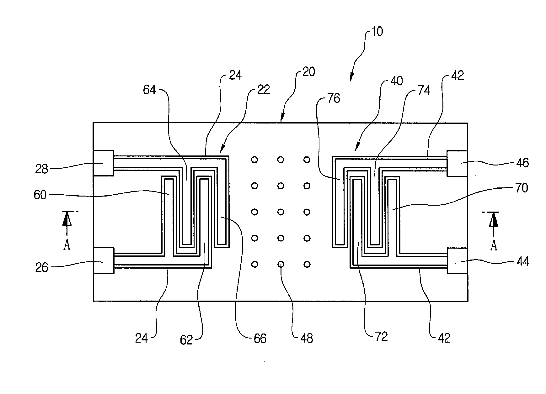
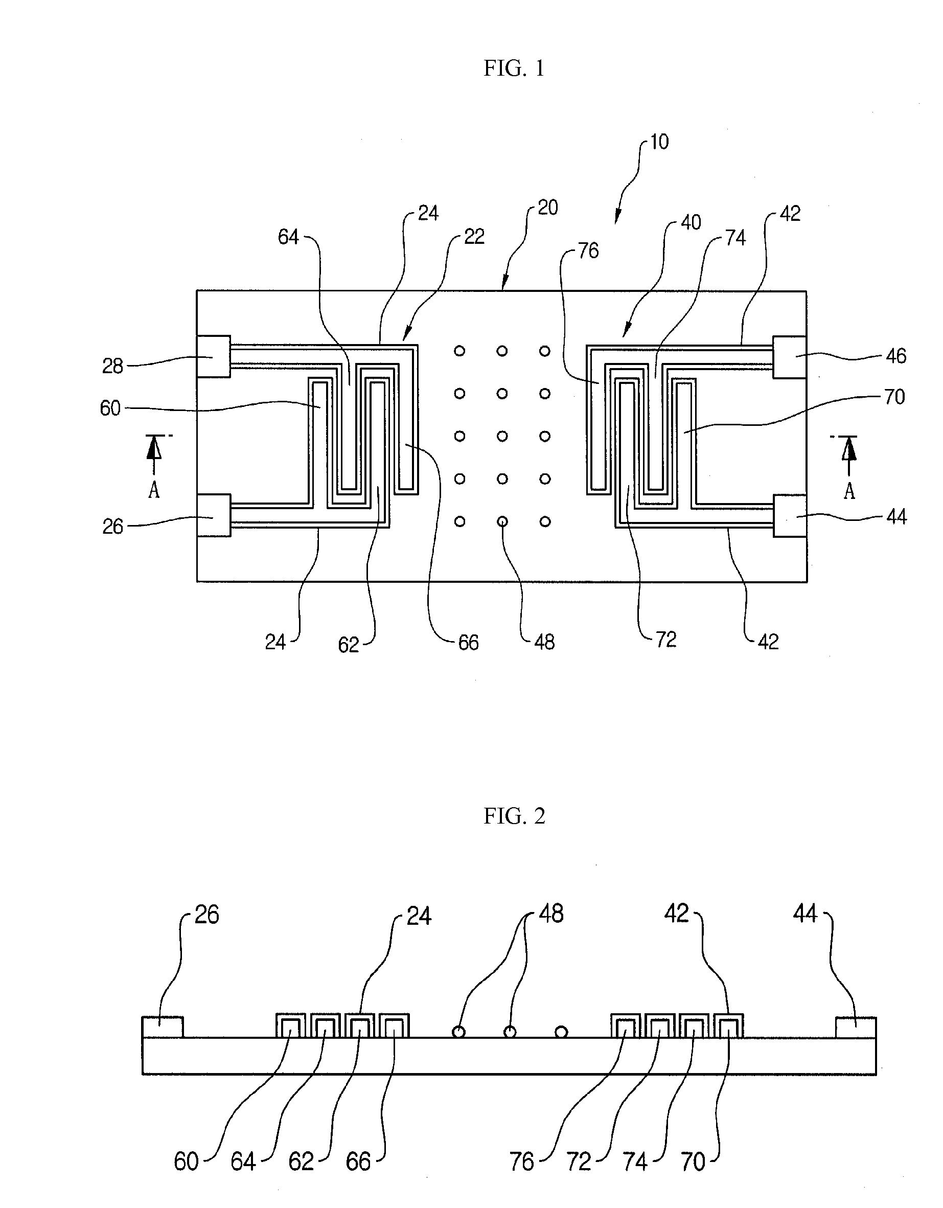
[0008]Exemplary embodiments provide a surface acoustic wave element, a surface acoustic wave device and methods for manufacturing the same, capable of effectively preventing leakage current from occurring when either applying electrical signals to the surface acoustic wave element or detecting electrical signals from the surface acoustic wave element.
[0033]In one exemplary embodiment, the target material communicating with the sensing area is disposed in a liquid and the first and second oxide films prevent a leakage current from flowing from the first plurality of electrodes and the second plurality of electrodes, respectively, to the liquid.
[0040]In one exemplary embodiment, the target material communicating with the sensing area is disposed in a liquid and the first and second oxide films prevent a leakage current from flowing from the first plurality of electrodes and the second plurality of electrodes, respectively, to the liquid.

Problems solved by technology

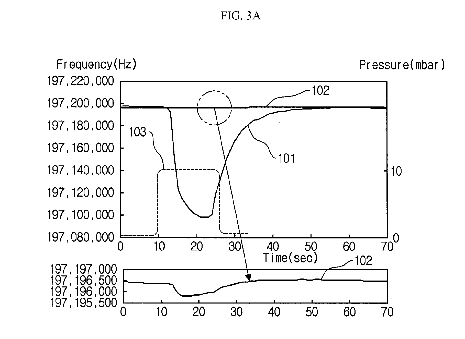
A leakage current may undesirably flow through the sample having the salt from the portions of the SAW where electrical signals are input to the SAW sensor or output from the SAW sensor.
When the leakage current occurs, a wave for oscillation or resonance is not be generated in the SAW sensor, resulting in the SAW sensor not being able to accurately sense the target material.

Method used


Image

  • Surface acoustic wave element, surface acoustic wave device and methods for manufacturing the same
  • Surface acoustic wave element, surface acoustic wave device and methods for manufacturing the same
  • Surface acoustic wave element, surface acoustic wave device and methods for manufacturing the same

Examples


Embodiment Construction

[0051]Exemplary embodiments now will be described more fully hereinafter with reference to the accompanying drawings. Exemplary embodiments may, however, be embodied in many different forms and should not be construed as limited to the embodiments set forth herein. Rather, these embodiments are provided so that this disclosure will be thorough and complete, and will fully convey the scope of the invention to those skilled in the art. Like reference numerals refer to like elements throughout.

[0052]It will be understood that when an element is referred to as being “on” another element, it can be directly on the other element or intervening elements may be present therebetween. In contrast, when an element is referred to as being “directly on” another element, there are no intervening elements present. As used herein, the term “and / or” includes any and all combinations of one or more of the associated listed items.

[0053]It will be understood that, although the terms first, second, thir...


PUM

PropertyMeasurementUnit
Shapeaaaaaaaaaa
Electrical conductoraaaaaaaaaa
Piezoelectricityaaaaaaaaaa

Abstract

A surface acoustic wave (“SAW”) element includes a substrate which is formed of a piezoelectric material, a plurality of first electrodes which are disposed on the substrate and separated from each other, a plurality of second electrodes which are disposed on the substrate and are separated from the first electrodes and are separated from each other, and oxide films which are disposed on the respective plurality of first electrodes and the plurality of second electrodes.

Description

CROSS-REFERENCE TO RELATED APPLICATIONS[0001]This application claims priority to Korean Patent Application No. 10-2008-0109042 filed on Nov. 4, 2008 and Korean Patent Application No. 10-2008-0135542 filed on Dec. 29, 2008, and all the benefits accruing therefrom under 35 U.S.C. §119, the contents of which in their entireties are herein incorporated by reference.BACKGROUND[0002]1) Field[0003]The general inventive concept relates to a surface acoustic wave (“SAW”) element, a SAW device and methods for manufacturing the same.[0004]2) Description of the Related Art[0005]A SAW sensor is, in general, a device that detects a target material in a sample using a piezoelectric material. An oscillation signal is applied to the SAW sensor. Using an interdigital transducer (“IDT”) electrode included in the SAW sensor, the oscillation signal is converted into a SAW, which is a mechanical wave, and vice versa.[0006]When the target material in the sample is bound to the surface of the SAW sensor, a...

Claims


Application Information

Patent Timeline
IPC IPC(8): H01L41/047H01L41/22
CPCG01N29/022G01N29/036G01N29/30G01N2291/0255G01N2291/0256G01N2291/0423H03H9/02645H03H9/1071H03H2250/00Y10T29/42
Inventor LEE, HUN JOOLEE, SOOSUKPARK, CHINSUNGKIM, KIEUN
Owner SAMSUNG ELECTRONICS CO LTD
Why Eureka
Try Eureka