Semiconductor device that include silicide layers

a technology of silicide layer and semiconductor, applied in the direction of semiconductor devices, semiconductor/solid-state device details, electrical equipment, etc., can solve the problems of high probability of overetching, difficult to form contacts on semiconductor thin films, and difficult to form contacts, so as to prevent defective contacts, reduce the total concentration of defects, and reduce the concentration of defects

Inactive Publication Date: 2005-04-19
SEMICON ENERGY LAB CO LTD
View PDF20 Cites 74 Cited by
  • Summary
  • Abstract
  • Description
  • Claims
  • Application Information

AI Technical Summary

Benefits of technology

[0017]In one embodiment, a top layer of interconnect metal is formed on the gate electrode. This top layer of interconnect metal may be connected with the metallization layer via at least one contact. This structure corresponds to Invention 2. For example, it can be a contact between the top layer of interconnect metal and the source or drain of each TFT (silicide layer). This structure is effective in preventing defective contacts between the quite thin silicide layer described in connection with FIGS. 2(A)-2(F) and the top layer of interconnect metal.
[0018]The active layer of the TFT needs to be quite thin because of the required characteristics. However, the present invention does not demand that the metallization layer be made quite thin, because the metallization layer in accordance with the present invention is intended to form a silicide layer in the active layer. Rather, the metallization layer may be made sufficiently thick. In the present invention, the whole silicide layer forming the source and drain is in contact with the metallization layer, forming an alloy. The metallization layer is in contact with the top layer of interconnect metal. The concentration of defects of the former is very low. Also, the concentration of defects of the latter is much lower than that of the structure of FIGS. 2(A)-2(F), because the metallization layer is sufficiently thick. Accordingly, the total concentration of defects is greatly reduced.
[0020]Generally, the gate layer forming the gate electrode and gate interconnect is isolated from the metallization layer forming the source and drain by an interlayer dielectric. Therefore, contact holes have been always required to make contacts between these two layers. Obviously, the freedom from the contact holes is advantageous to the circuit arrangement.
[0025]A fabrication step of forming a more heavily doped region may be performed between the steps (2) and (3). This heavily doped region is of the same conductivity type as the doped regions formed by the above-described process steps. Thus, a double-implant lightly doped drain (DI-LDD) structure can be obtained. This step may be carried out after the step (3). In this case, the implants may not be done up to a desired depth, depending on the thickness of the metallization layer. If this step is performed after the step (5), implants can be carried out into other than the double-implant lightly doped drain structure without difficulty.

Problems solved by technology

These requirements become more important and technical difficulties arise as the circuit device density increases.
However, it is quite difficult to form contacts on a semiconductor thin film as thin as hundreds of Angstroms.
During fabrication of contact holes, overetching is highly likely to occur, forming holes or pits in the semiconductor holes.
This phenomenon takes place, because the etch rates of silicon oxide and silicon nitride generally used as interlayer dielectrics and the etch rate of silicon (especially, in the case of dry etching) used as a semiconductor thin film are not very high.
However, the problem cannot be solved simply by devising the circuit arrangement because of design rule problems.
However, the problems produced where contact holes are created can be hardly solved, because the etch rates of silicides and silicon oxide or silicon nitride are not sufficiently high where a dry etching method is used.
With this method, if the etch rates of silicon nitride and the active layer are not sufficiently high where the interlayer dielectric is etched, it is difficult to detect the end point of the etching, since the silicon nitride layer is approximately 10 times as thick as the active layer.
Other problems may arise, depending on circuits.
Contacts tend to produce many defects and have large resistivities.
Furthermore, the silicide layer is very thin, producing many defects at the contacts, though the possibility of overetching decreases.
Consequently, the contact holes are required to have sufficient spread, which is an obstacle in achieving higher circuit density.

Method used


Image

  • Semiconductor device that include silicide layers
  • Semiconductor device that include silicide layers
  • Semiconductor device that include silicide layers

Examples


embodiment 1

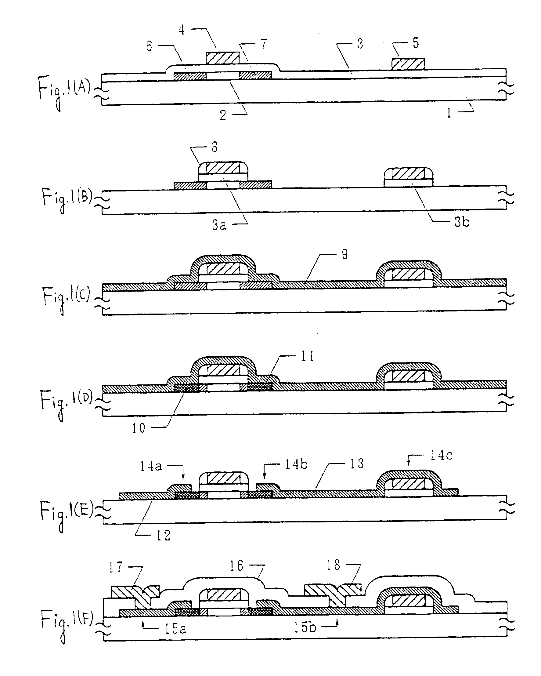
[0039]FIGS. 1(A)-1(F) schematically illustrate a process sequence for fabricating TFTs in accordance with the present embodiment. Although these are n-channel TFTs, it is obvious that p-channel TFTs can be manufactured also by forming the source / drain regions out of a p-type semiconductor. The TFTs in accordance with the present embodiment can be disposed at pixels of liquid crystal displays, used in peripheral circuits, in image sensors, and in other integrated circuits.

[0040]In the present embodiment, a substrate 1 is made of a glass substrate coated with a silicon oxide film (not shown) having a thickness of 2000 Å. The coating can be made by sputtering or plasma-assisted CVD (PCVD). Then, an amorphous silicon film is formed to a thickness of 500 Å by PCVD. The method of forming this amorphous silicon film and its film thickness are determined according to the manner in which the present invention is practiced, and no limitations are imposed on them. Also, a crystalline silicon f...

embodiment 2

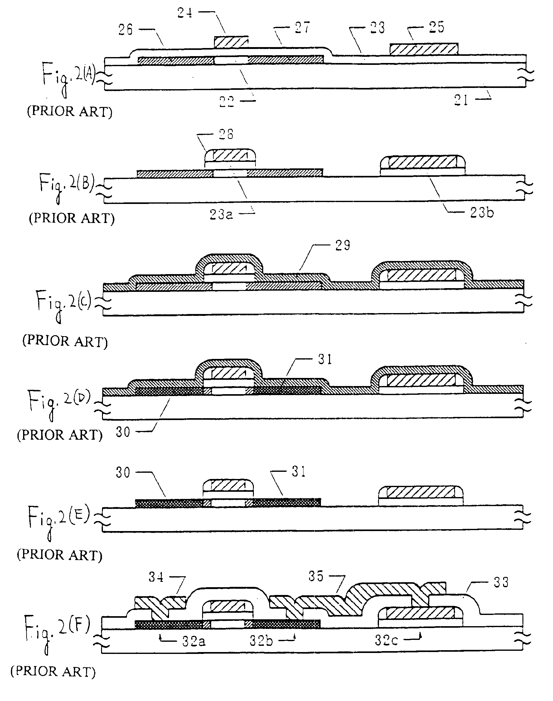
[0055]FIGS. 3(A)-3(F) schematically illustrate a process sequence for fabricating TFTs in accordance with the present invention. What are fabricated in the present embodiment are n-channel TFTs, but it is obvious that p-channel TFTs can be manufactured by forming the source / drain regions out of a p-type semiconductor. The TFTs in accordance with the present embodiment can be disposed at pixels of liquid crystal displays, used in peripheral circuits, in image sensors, and in other integrated circuits.

[0056]In the present embodiment, a substrate 41 is made of a glass substrate coated with a silicon oxide film (not shown) having a thickness of 2000 Å. Islands of a crystalline silicon film (active layer) 42 are formed on the substrate. A silicon oxide film 43 becoming a gate insulator layer is formed to a thickness of 1200 Å over the crystalline silicon film. Then, a gate electrode 44 and a gate interconnect 45 are formed out of a polycrystalline phosphorus-doped silicon film. Phosphoru...

embodiment 3

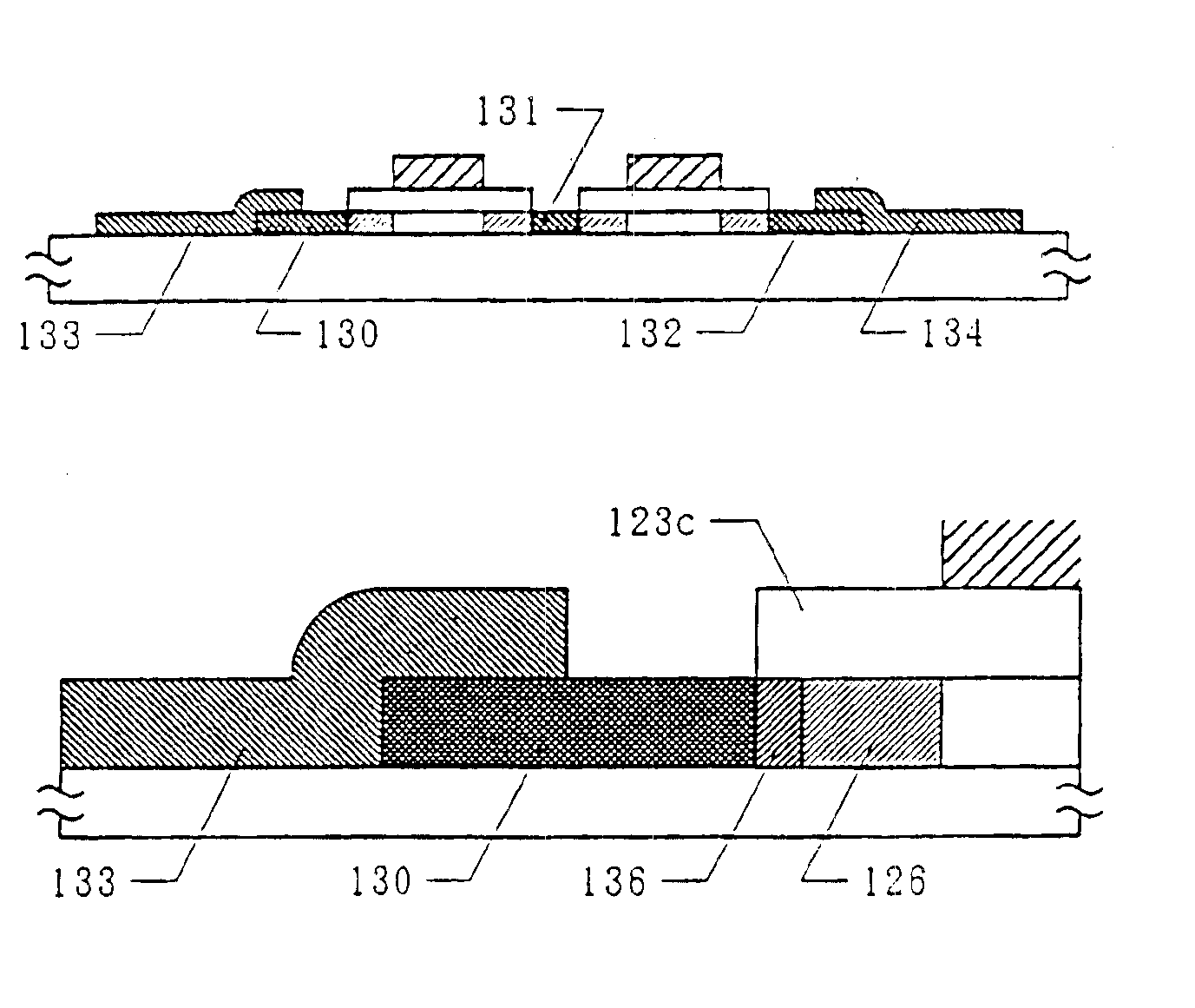
[0062]FIGS. 4(A)-4(F) schematically illustrate a process sequence for fabricating TFTs in accordance with the present embodiment. In this embodiment, a substrate 61 is made of a glass substrate coated with a silicon oxide film (not shown) having a thickness of 2000 Å. Islands of a crystalline silicon film (active layer) 62 are formed on the substrate. A silicon oxide film 63 becoming a gate insulator layer is formed to a thickness of 1200 Å over the crystalline silicon film. Then, a gate electrode 64 and a gate interconnect 65 are formed out of a polycrystalline phosphorus-doped silicon film. Phosphorus ions are implanted as dopants into the active layer 62 to impart the n-type conductivity. During this process step, the gate electrode 64 acts as a mask, and doped regions 66 and 67 are formed in a self-aligned manner but with a low dopant concentration of 1×10¹⁷ to 1019 atoms / cm3 (FIG. 4(A)).

[0063]In the same way as in Embodiment 1, sidewalls 68 are formed on the sidewalls of the ga...


PUM


Abstract

There is disclosed a method of fabricating TFTs having reduced interconnect resistance by having improved contacts to source / drain regions. A silicide layer is formed in intimate contact with the source / drain regions. The remaining metallization layer is selectively etched to form a contact pad or conductive interconnects.

Description

CROSS-REFERENCE TO RELATED APPLICATIONS[0001]This application is a divisional application of U.S. application Ser. No. 08 / 958,568, filed on Oct. 28, 1997, now abandoned, which claims the benefit of a foreign priority application filed in Japan on Oct. 31, 1996 as Application No. 08-307443, both of which are incorporated by reference.BACKGROUND OF THE INVENTION[0002]1. Field of the Invention[0003]The present invention relates to a TFT structure or a semiconductor integrated circuit construction having TFTs and to a method of fabricating such a structure. Especially, the invention relates to conductive interconnects for TFTs or for a semiconductor integrated circuit having TFTs Also, the invention relates to a method of forming such interconnects.[0004]2. Description of the Related Art[0005]Techniques for using TFTs (thin-film transistors) in an integrated circuit such as an active matrix liquid crystal display or image sensor fabricated on a glass substrate have been well known. Maki...

Claims


Application Information

Patent Timeline
Patent Type & Authority Patents(United States)
IPC IPC(8): H01L21/70H01L29/66H01L29/45H01L27/12H01L21/336H01L21/02H01L29/786H01L21/84H01L29/40H01L29/78H01L21/77
CPCH01L21/28518H01L27/12H01L29/458H01L27/124H01L29/78621H01L29/78645H01L29/66757H01L2029/7863
Inventor OHTANI, HISASHIFUJIMOTO, ETSUKO
Owner SEMICON ENERGY LAB CO LTD
Why Eureka
Try Eureka