Touch-sensing substrate, color filter substrate and touch-sensing liquid crystal display

a technology color filter substrate, which is applied in the field of touch sensing substrate, color filter substrate and touch sensing liquid crystal display, can solve the problems of complicated fabrication and low resolution, the capacitive sensing layer easily affects the overall transmittance of the color filer substrate, etc., and achieves the effect of improving the overall transmittance and improving the sheet resistan

Active Publication Date: 2010-05-06
AU OPTRONICS CORP
View PDF9 Cites 57 Cited by
  • Summary
  • Abstract
  • Description
  • Claims
  • Application Information

AI Technical Summary

Benefits of technology

[0010]The present invention provides a color filter substrate which uses a plurality of patterned conductive layers to improve the increased sheet resistance due to reduction in thickness of a transparent conductive layer and thereby provides better transmittance.

Problems solved by technology

The dual side design is easier in fabrication but has limitation in terms of thickness and resolution.
The single side design provides simpler structure than the dual side design but also has the problems of complicated fabrication and low resolution.
However, thickness of the capacitive sensing layer easily affects overall transmittance of the color filer substrate.
The aforesaid method, however, increases the sheet resistance of the conductive film layer in the capacitive sensing layer and thereby reduces the strength of sensing signals.
Furthermore, the touch panel of the single side design in the conventional technology also encounters the same problem.

Method used


Image

  • Touch-sensing substrate, color filter substrate and touch-sensing liquid crystal display
  • Touch-sensing substrate, color filter substrate and touch-sensing liquid crystal display
  • Touch-sensing substrate, color filter substrate and touch-sensing liquid crystal display

Examples


first embodiment

The First Embodiment

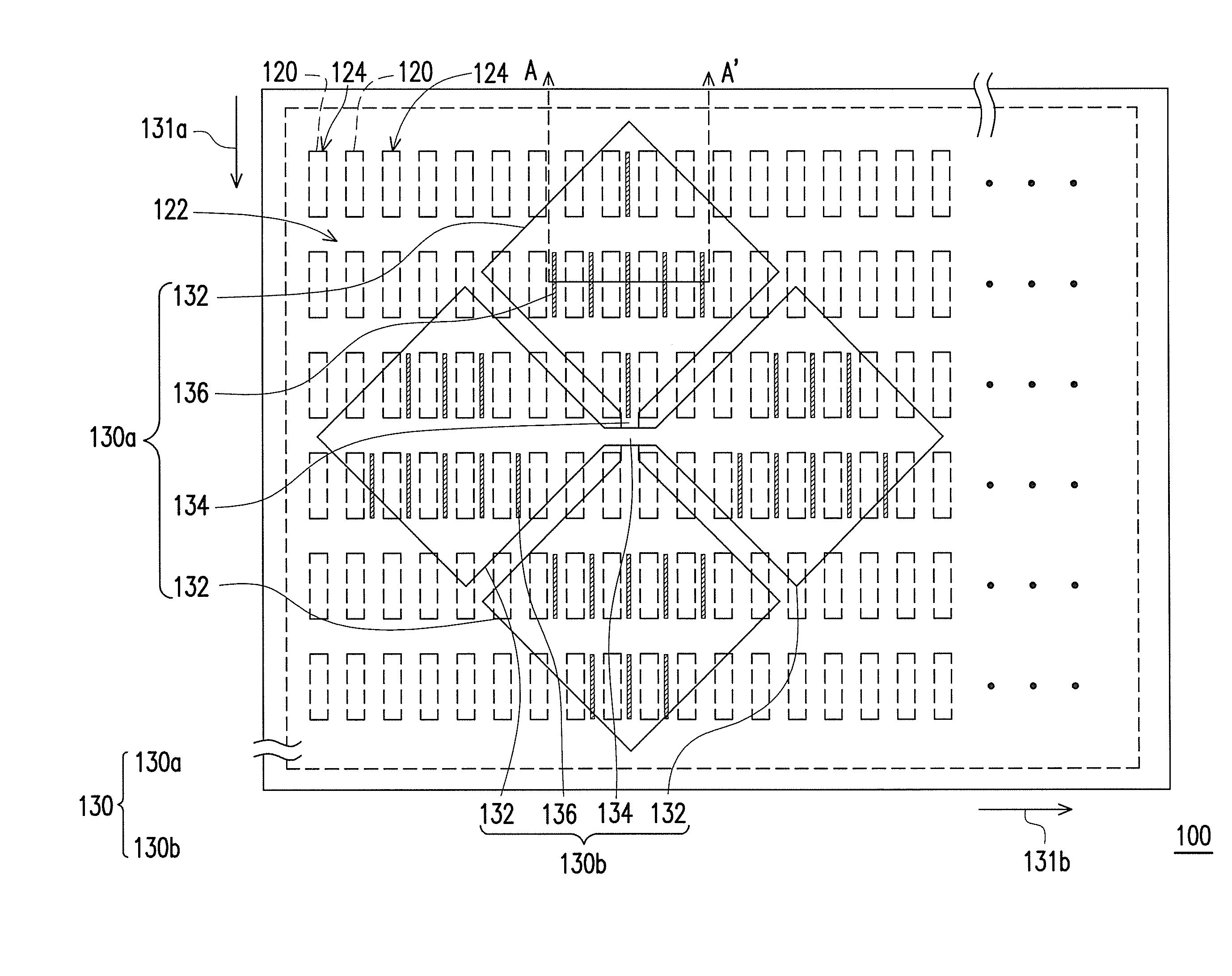
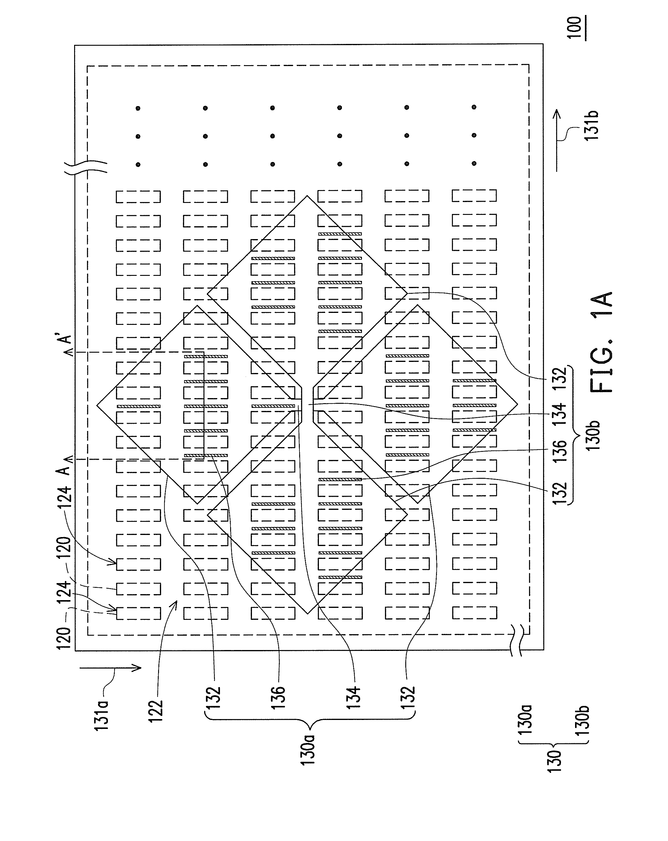
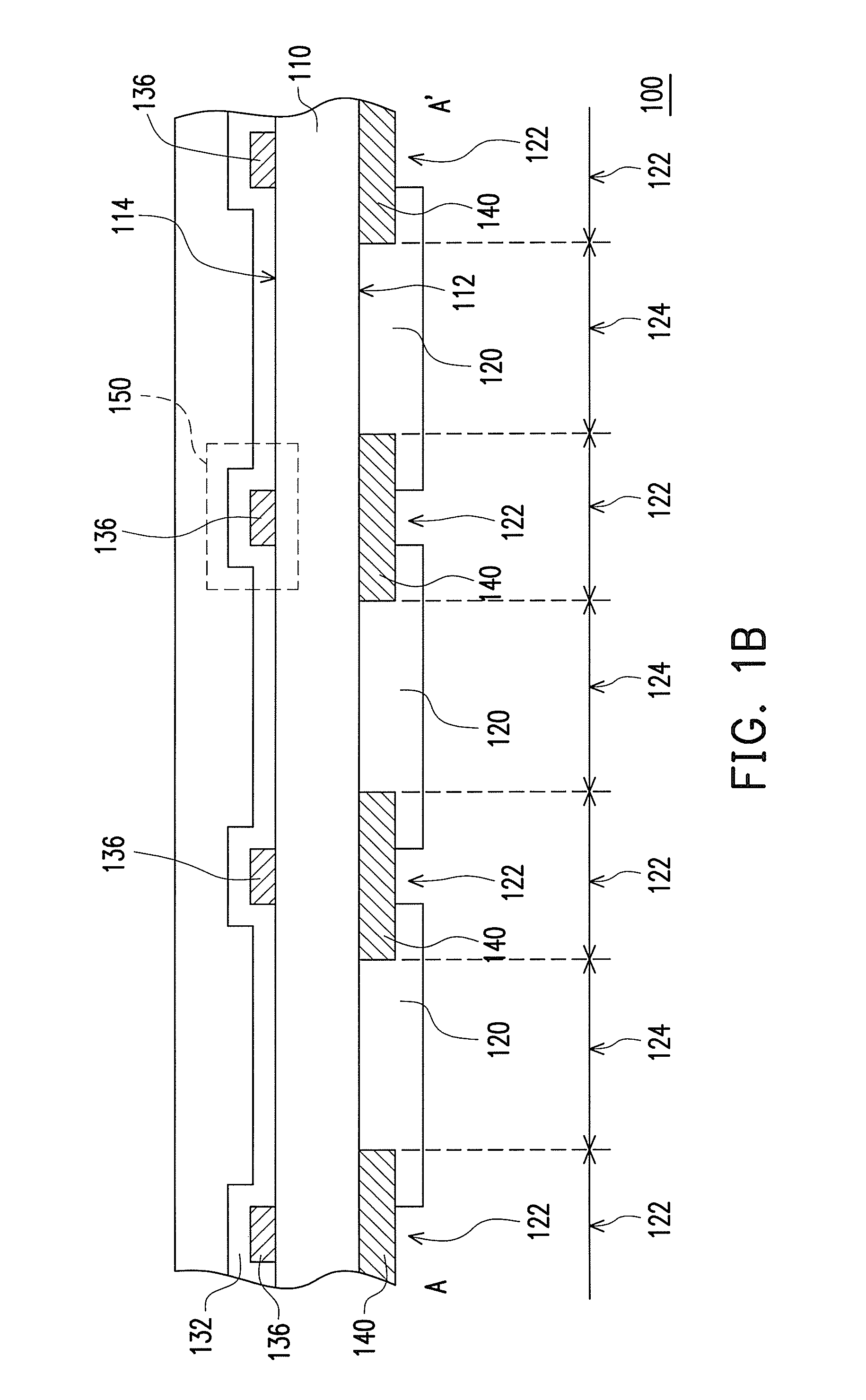
[0039]FIG. 1A is a partial top view of a color filter substrate according to one embodiment of the present invention. FIG. 1B is a cross-sectional view of the color filter substrate in FIG. 1A taken along a line AA′. A region in FIG. 1A depicted with dotted lines is a perspective view of a first surface of the color filter substrate. For simplicity of illustration, FIG. 1A mainly shows schematic views of display regions, patterned color filter layers, a separated region, and sensing serials, omitting other possible layers. From a comparison of FIG. 1A and FIG. 1B, the color filter substrate 100 is a touch-sensing color filter substrate of a dual side design. A detailed illustration on the structure of the color filter substrate 100 is given below

[0040]Referring to FIG. 1A and FIG. 1B, the color filter substrate 100 of the present embodiment includes a substrate 110, a plurality of patterned color filter layers 120 and a plurality of sensing serials 130. In the pr...

second embodiment

The Second Embodiment

[0067]A touch-sensing substrate of the present embodiment adopts the design concept similar to the above-mentioned color filter substrates except that the touch-sensing substrate is an opposite substrate (opposite to the transistor array substrate) and provides touch-sensing functionality. In other words, only the sensing serials are arranged on the opposite substrate, the above-mentioned patterned color filter layers are correspondingly disposed on the display regions of the transistor array substrate. The relationship of each of the components of the touch-sensing substrate is detailed in the following.

[0068]FIG. 5 is a partial top view of a touch-sensing substrate of the present invention. For simplicity of illustration, FIG. 5 mainly depicts structures of display regions and sensing serials, omitting other possible layers. Referring to FIG. 5, a touch-sensing substrate 400 of the present embodiment includes a substrate 410 and a plurality of sensing serials ...


PUM

PropertyMeasurementUnit
widthaaaaaaaaaa
widthaaaaaaaaaa
conductiveaaaaaaaaaa

Abstract

A color filter substrate including a substrate, a plurality of patterned color filter layers, and a plurality of sensing serials is provided. The substrate has a first surface and a second surface opposite to the first surface. The substrate includes a plurality of display regions arranged in array and a separated region located between the display regions. The patterned color filter layers are arranged in array on the first surface and corresponding to the display regions. The sensing serials are arranged on the second surface and insulated from each other. Each sensing serial includes a plurality of sensing pads; a plurality of bridging lines, each connected with two adjacent sensing pads; a plurality of patterned conductive layers stacked and electrically connected with the sensing pads. The position of the patterned conductive layers is corresponding to the separated region. A touch-sensing liquid crystal display and a touch-sensing substrate are also provided.

Description

CROSS-REFERENCE TO RELATED APPLICATION[0001]This application claims the priority benefit of Taiwan application serial no. 97142742, filed Nov.5, 2008. The entirety of the above-mentioned patent application is hereby incorporated by reference herein and made a part of specification.BACKGROUND OF THE INVENTION[0002]1. Field of the Invention[0003]The present invention relates to a touch-sensing substrate, and more particularly, to a touch-sensing substrate which may be integrated into a color filter substrate or a touch sensing liquid crystal display.[0004]2. Description of Related Art[0005]With the rapid development and application of information technology, wireless mobile communication, and informational household appliances, a good number of informational products are now using a touch panel as an input device instead of a conventional input device such as a keyboard or a mouse, wherein a touch-sensing display has become one of the most popular products on the current market.[0006]...

Claims


Application Information

Patent Timeline
Patent Type & Authority Applications(United States)
IPC IPC(8): G06F3/041G02B5/22G02F1/1335
CPCG02B5/201G02F1/13338G02F1/133512G02F1/133514G06F3/0412G06F3/044G06F2203/04111G06F3/0443G06F3/0446
Inventor CHIEN, YU-FENGYANG, TUN-CHUNLEE, SEOK-LYULHUANG, WEI-MINGWU, YUAN-CHUN
Owner AU OPTRONICS CORP
Why Eureka
Try Eureka