Resistance variable memory apparatus

a memory apparatus and resistance variable technology, applied in the field of resistance variable memory apparatus, can solve the problems of difficult miniaturization, long programming time, and limit in the reduction of its siz

Active Publication Date: 2010-05-06
PANASONIC SEMICON SOLUTIONS CO LTD
View PDF5 Cites 67 Cited by
  • Summary
  • Abstract
  • Description
  • Claims
  • Application Information

AI Technical Summary

Benefits of technology

[0038]The present invention has the above described configuration and achieves advantages described below. That is, it is possible to provide a resistance variable memory apparatus which is capable of surely preventing an incorrect opera

Problems solved by technology

It is pointed out that the flash memory has a problem that, since the flash memory has a structure in which the electric charges are accumulated in a high electric field on the floating gate, there is a limitation in reduction of its size and it is difficult to achieve miniaturization which is required to achieve a larger capacity.
In addition, in the flash memory, specified blocks must be erased all at once

Method used


Image

  • Resistance variable memory apparatus
  • Resistance variable memory apparatus
  • Resistance variable memory apparatus

Examples


embodiment 1

[0216]Hereinafter, a resistance variable memory apparatus according to Embodiment 1 of the present invention will be described.

Configuration

[0217]FIG. 8 is a block diagram showing an example of a schematic configuration of the resistance variable memory apparatus according to Embodiment 1 of the present invention. Hereinafter, the configuration of the resistance variable memory apparatus 100 of this embodiment will be described with reference to FIG. 8.

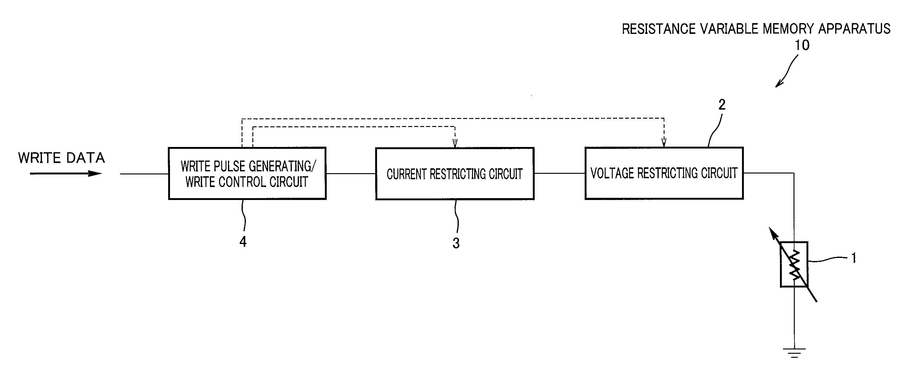
[0218]As shown in FIG. 8, the resistance variable memory apparatus 100 comprises a resistance variable element 110, a nMOS 120 (voltage restricting active element), a pMOS 130 (current restricting active element), and a write pulse generating / write control circuit 140 (controller).

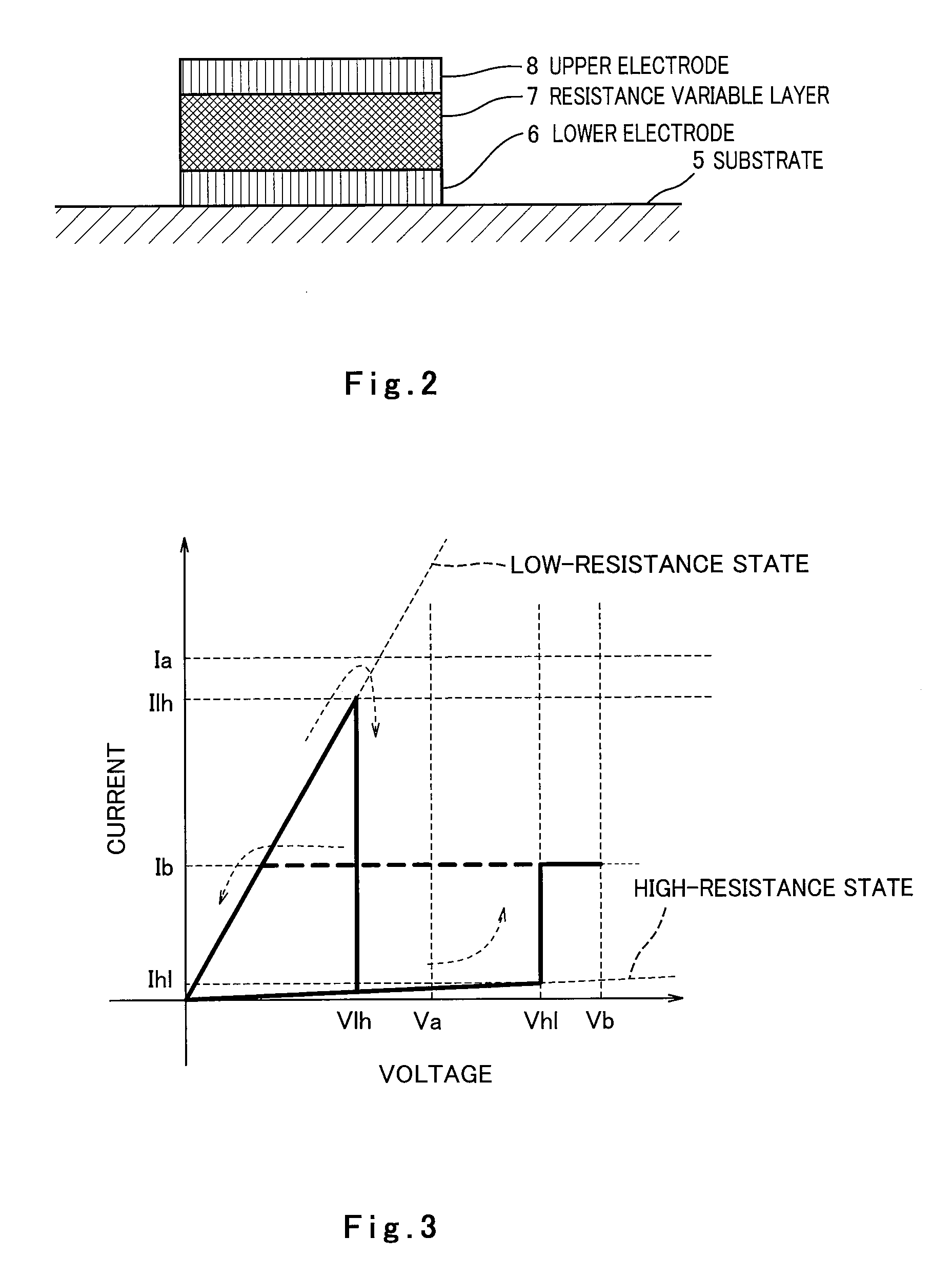
[0219]The resistance variable element 110 has a configuration similar to that of the resistance variable element 1 of FIG. 1 and has a characteristic shown in FIG. 3. The resistance variable element 110 has a first terminal 111 and a second terminal 112. The...

embodiment 2

[0249]Hereinafter, a resistance variable memory apparatus according to Embodiment 2 of the present invention will be described.

Configuration

[0250]FIG. 15 is a block diagram showing an example of a schematic configuration of the resistance variable memory apparatus according to Embodiment 2 of the present invention. Hereinafter, the configuration of a resistance variable memory apparatus 200 of this embodiment will be described with reference to FIG. 15.

[0251]As shown in FIG. 15, the resistance variable memory apparatus 200 comprises a resistance variable element 210, a nMOS 220 (voltage restricting active element), a pMOS 230 (current restricting active element), a write pulse generating / write control circuit 240 (controller), a voltage source 241, a nMOS 250, a pMOS 260, a series resistor 270, and a parallel resistor 280.

[0252]Since the resistance variable element 210, the nMOS 220, the pMOS 230, and the write pulse generating / write control circuit 240 are similar to the resistance...

embodiment 3

Configuration

[0277]FIG. 18 is a block diagram showing an example of a schematic configuration of a resistance variable memory apparatus according to Embodiment 3 of the present invention. Hereinafter, the configuration of a resistance variable memory apparatus 300 of this embodiment will be described with reference to FIG. 18.

[0278]As shown in FIG. 18, the resistance variable memory apparatus 300 comprises an address input circuit 302, a read / write control circuit 304, a write pulse timing generating circuit 306, a write data determiner circuit 308, a data input / output circuit 310, a write pulse drive circuit 312 (current restricting circuit), a read circuit 318, an electric power supply circuit 320, a row decoder 330, a word driver 332, a column decoder 334, and a memory array 336.

[0279]The write pulse drive circuit 312 includes a first drive circuit 314 (current capacity: Ia) and a second drive circuit 316 (current capacity: Ib).

[0280]The electric power supply circuit 320 includes...


PUM


Abstract

A resistance variable memory apparatus (10) of the present invention comprises a resistance variable element (1) which is switched to a high-resistance state when a voltage exceeds a first voltage and is switched to a low-resistance state when the voltage exceeds a second voltage, a controller (4), a voltage restricting active element (2) which is connected in series with the resistance variable element (1); and a current restricting active element which is connected in series with the resistance variable element (1) via the voltage restricting active element (2), and the controller (4) is configured to control the current restricting active element (3) so that a product of a current and a first resistance value becomes a first voltage or larger and to control the voltage restricting active element (2) so that the voltage between electrodes becomes smaller than a second voltage when the element is switched to the high-resistance state, while the controller (4) is configured to control the current restricting active element (3) so that an absolute value of a product of the current and the second resistance value becomes the second voltage or larger and an absolute value of a product of the current and the first resistance value becomes smaller than the first voltage, when the element is switched to the low-resistance state.

Description

TECHNICAL FIELD[0001]The present invention relates to a resistance variable memory apparatus. More particularly, the present invention relates to a resistance variable memory apparatus using a resistance variable element which is switchable to a high-resistance state and to a low-resistance state in response to applied electric pulses which are identical in polarity and are different in voltage level.BACKGROUND ART[0002]Nonvolatile memory apparatuses are widely used to be built into a variety of portable hardware such as cellular phones and digital cameras, and their uses have been spreading at a high pace. In recent years, in many occasions, audio data or image data have been used, and hence there has been a strong demand for nonvolatile memory apparatuses which have a larger capacity and are operable at a higher speed. Besides, in fields of nonvolatile memory apparatuses for use with portable hardware, there has been a further demand for lower electric power consumption.[0003]At p...

Claims


Application Information

Patent Timeline
IPC IPC(8): G11C11/00G11C5/14
CPCG11C8/08G11C13/0028G11C13/003G11C13/0038G11C2213/79G11C2013/009G11C2213/15G11C2213/74G11C2213/76G11C13/0069
Inventor KATOH, YOSHIKAZUSHIMAKAWA, KAZUHIKO
Owner PANASONIC SEMICON SOLUTIONS CO LTD
Why Eureka
Try Eureka