Photovoltaic device

a photovoltaic and device technology, applied in the direction of basic electric elements, semiconductor devices, electrical equipment, etc., can solve the problems of limiting the applications to which solar cells may be suited, preventing solar cells from becoming a mainstream energy source, and the cost of producing solar cells, so as to achieve the effect of increasing efficiency

Active Publication Date: 2010-06-03
ALTA DEVICES INC
View PDF61 Cites 67 Cited by
  • Summary
  • Abstract
  • Description
  • Claims
  • Application Information

AI Technical Summary

Problems solved by technology

Nevertheless, the currently high cost of producing solar cells relative to the low efficiency levels of contemporary devices is preventing solar cells from becoming a mainstream energy source and limiting the applications to which solar cells may be suited.

Method used


Image

  • Photovoltaic device
  • Photovoltaic device
  • Photovoltaic device

Examples


Embodiment Construction

[0029]Embodiments of the present invention provide techniques and apparatus for converting electromagnetic radiation, such as solar energy, into electric energy with increased efficiency when compared to conventional solar cells.

An Exemplary Thin Absorber Layer

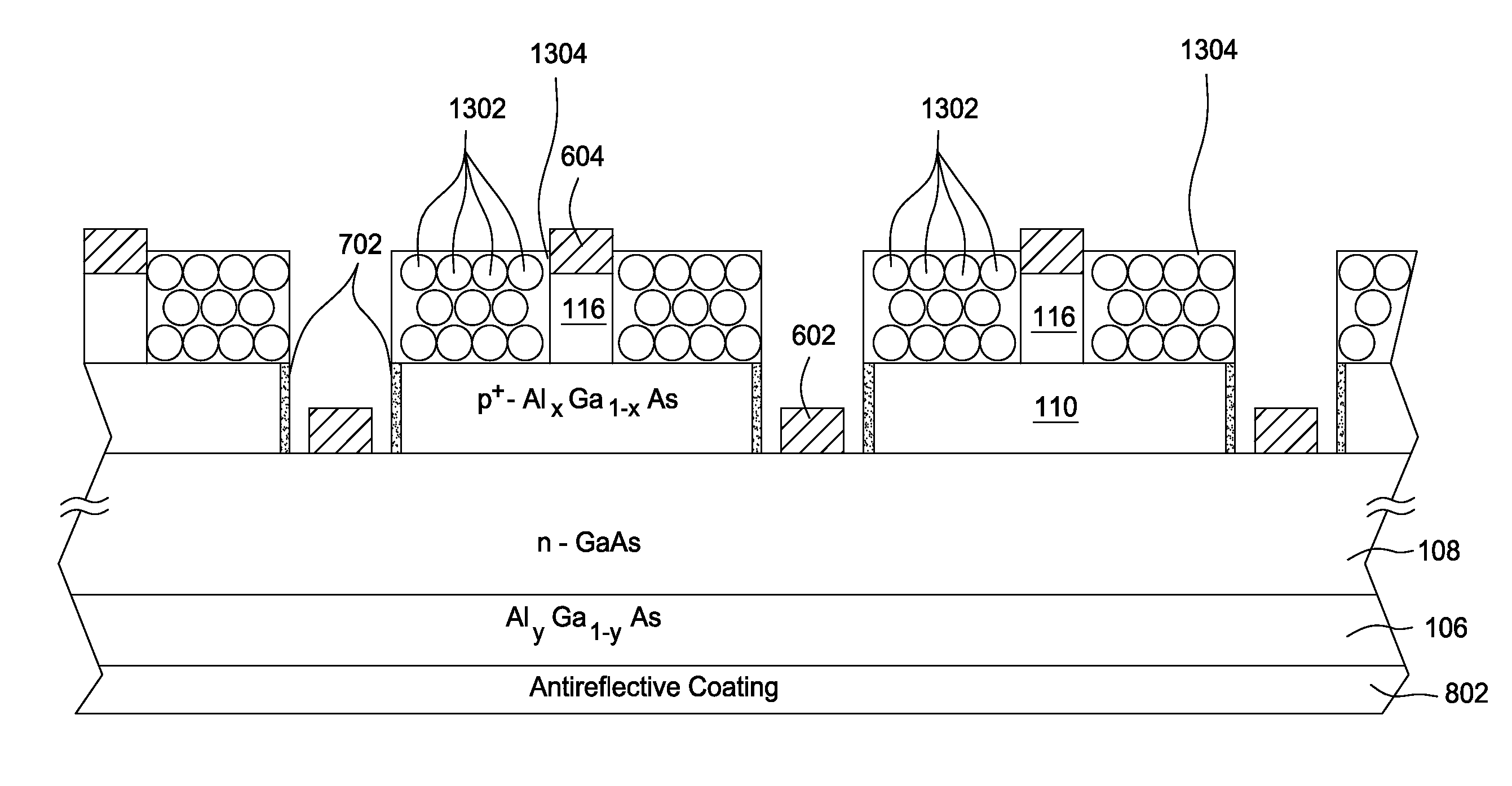
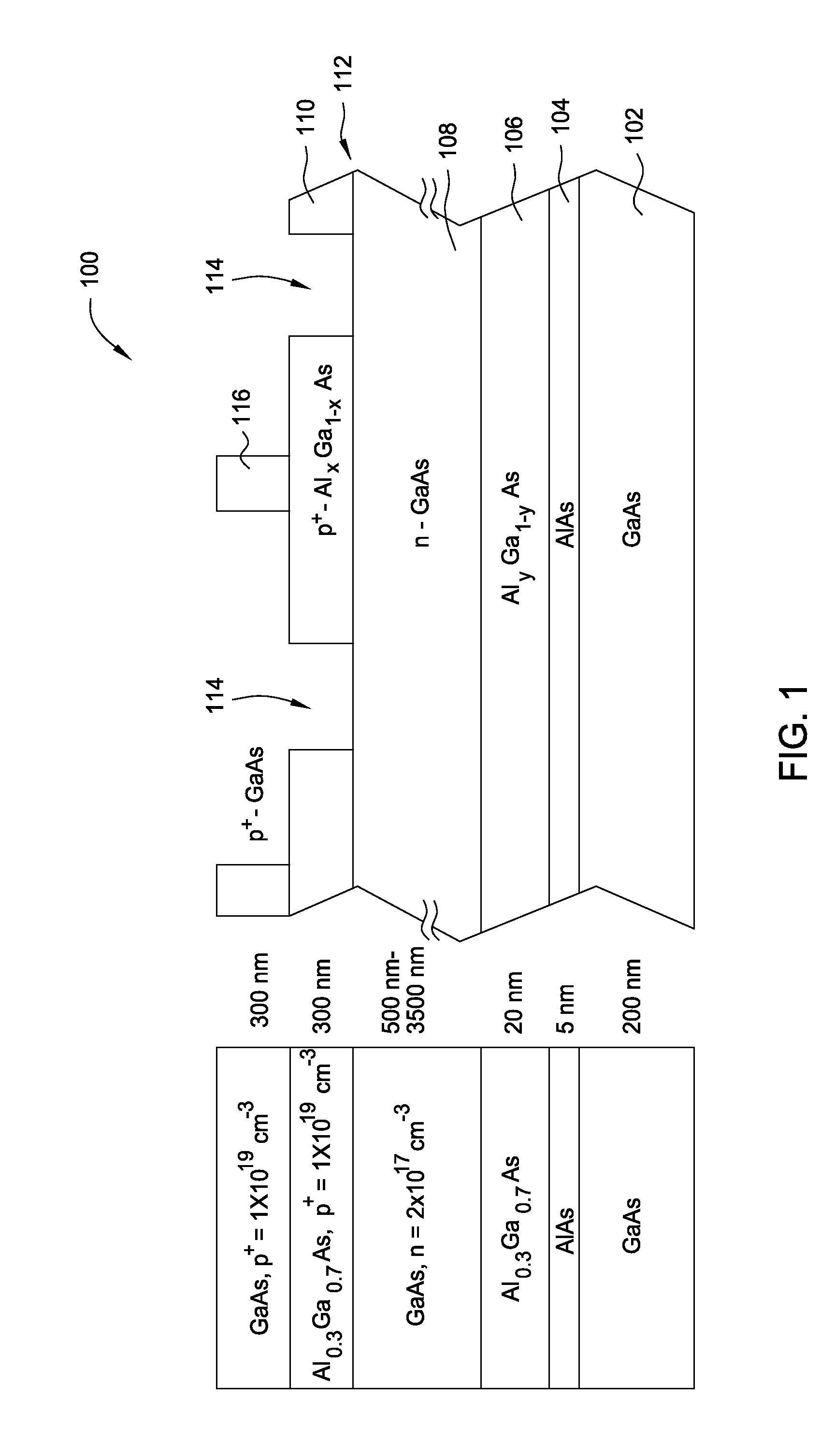
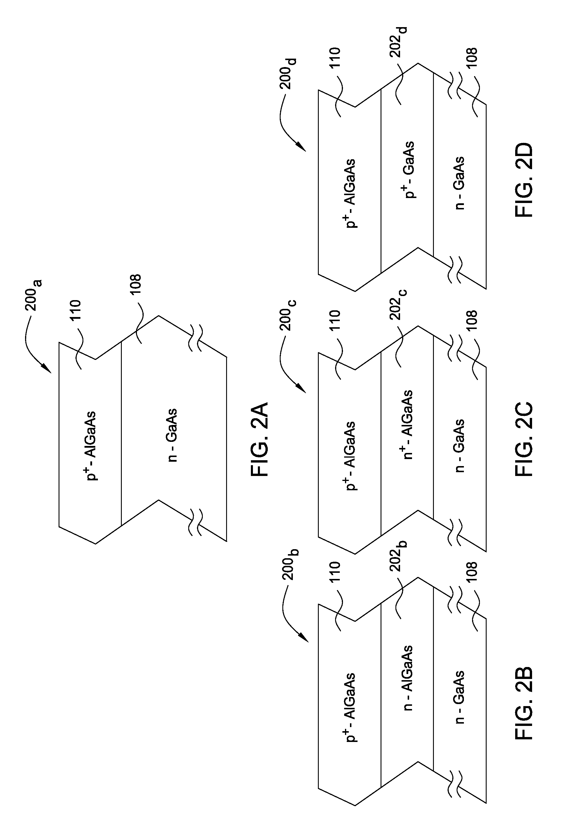
[0030]FIG. 1 illustrates various epitaxial layers of a photovoltaic (PV) unit 100 in cross-section during fabrication. The various layers may be formed using any suitable method for semiconductor growth, such as molecular beam epitaxy (MBE) or metalorganic chemical vapor deposition (MOCVD), on a substrate (not shown).

[0031]To form the PV unit 100, one or more buffer layers may be formed on the substrate. The purpose of the buffer layer(s) is to provide an intermediary between the substrate and the semiconductor layers of the final PV unit that can accommodate their different crystallographic structures as the various epitaxial layers are formed. Having a thickness of about 200 nm, for example, a buffer layer 102 may comprise a...


PUM


Abstract

Methods and apparatus are provided for converting electromagnetic radiation, such as solar energy, into electric energy with increased efficiency when compared to conventional solar cells. A photovoltaic (PV) unit, according to embodiments of the invention, may have a very thin absorber layer produced by epitaxial lift-off (ELO), all electrical contacts positioned on the back side of the PV device to avoid shadowing, and / or front side and back side light trapping employing a diffuser and a reflector to increase absorption of the photons impinging on the front side of the PV unit. Several PV units may be combined into PV banks, and an array of PV banks may be connected to form a PV module with thin strips of metal or conductive polymer applied at low temperature. Such innovations may allow for greater efficiency and flexibility in PV devices when compared to conventional solar cells.

Description

CROSS-REFERENCE TO RELATED APPLICATIONS[0001]This application claims benefit of U.S. Provisional Patent Application Ser. No. 61 / 107,954 filed Oct. 23, 2008, which is herein incorporated by reference in its entirety.BACKGROUND[0002]1. Technical Field[0003]Embodiments of the present invention generally relate to photovoltaic (PV) devices, such as solar cells, with increased efficiency and greater flexibility and methods for fabricating the same.[0004]2. Description of the Related Art[0005]As fossil fuels are being depleted at ever-increasing rates, the need for alternative energy sources is becoming more and more apparent. Energy derived from wind, from the sun, and from flowing water offer renewable, environment-friendly alternatives to fossil fuels, such as coal, oil, and natural gas. Being readily available almost anywhere on Earth, solar energy may someday be a viable alternative.[0006]To harness energy from the sun, the junction of a solar cell absorbs photons to produce electron...

Claims


Application Information

Patent Timeline
Patent Type & Authority Applications(United States)
IPC IPC(8): H01L31/00
CPCH01L31/0236H01L31/0735H01L31/0304Y02E10/544Y02E10/52H01L31/02363Y02E10/547H01L31/042H01L31/06H01L31/022441H01L31/03046H01L31/065H01L31/0682H01L31/0693H01L31/056Y02E10/50
Inventor KIZILYALLI, ISIK C.ARCHER, MELISSAATWATER, HARRYGMITTER, THOMAS J.HE, GANGHEGEDUS, ANDREASHIGASHI, GREGG
Owner ALTA DEVICES INC
Why Eureka
Try Eureka