Display device and method of driving the same

Active Publication Date: 2010-06-03
SAMSUNG DISPLAY CO LTD
View PDF9 Cites 3 Cited by
  • Summary
  • Abstract
  • Description
  • Claims
  • Application Information

AI Technical Summary

Benefits of technology

[0036]According to exemplary embodiments of the present invention, even if threshold voltages of driving transistors of pixels are not uniform, the luminance of the pixels

Problems solved by technology

The amorphous silicon TFT, however, has a difficulty in providing large increases in a display area of a display element due to low electron mobility.
This becomes a major factor that shortens the lifetime of the organic light emitting device.
In a process of forming an active layer with polysilicon, however, due to characteristics of a semiconductor that is included in the TFT, it is not easy to uniformly form the polysilicon TFT within

Method used


Image

  • Display device and method of driving the same
  • Display device and method of driving the same
  • Display device and method of driving the same

Examples


Embodiment Construction

[0051]Exemplary embodiments of the present invention will be described more fully hereinafter with reference to the accompanying drawings, in which exemplary embodiments of the present invention are shown. As those of ordinary skill in the art would realize, the described exemplary embodiments may be modified in various different ways, all without departing from the spirit or scope of the present invention.

[0052]First, an organic light emitting device according to an exemplary embodiment of the present invention will be described with reference to FIGS. 1 and 2.

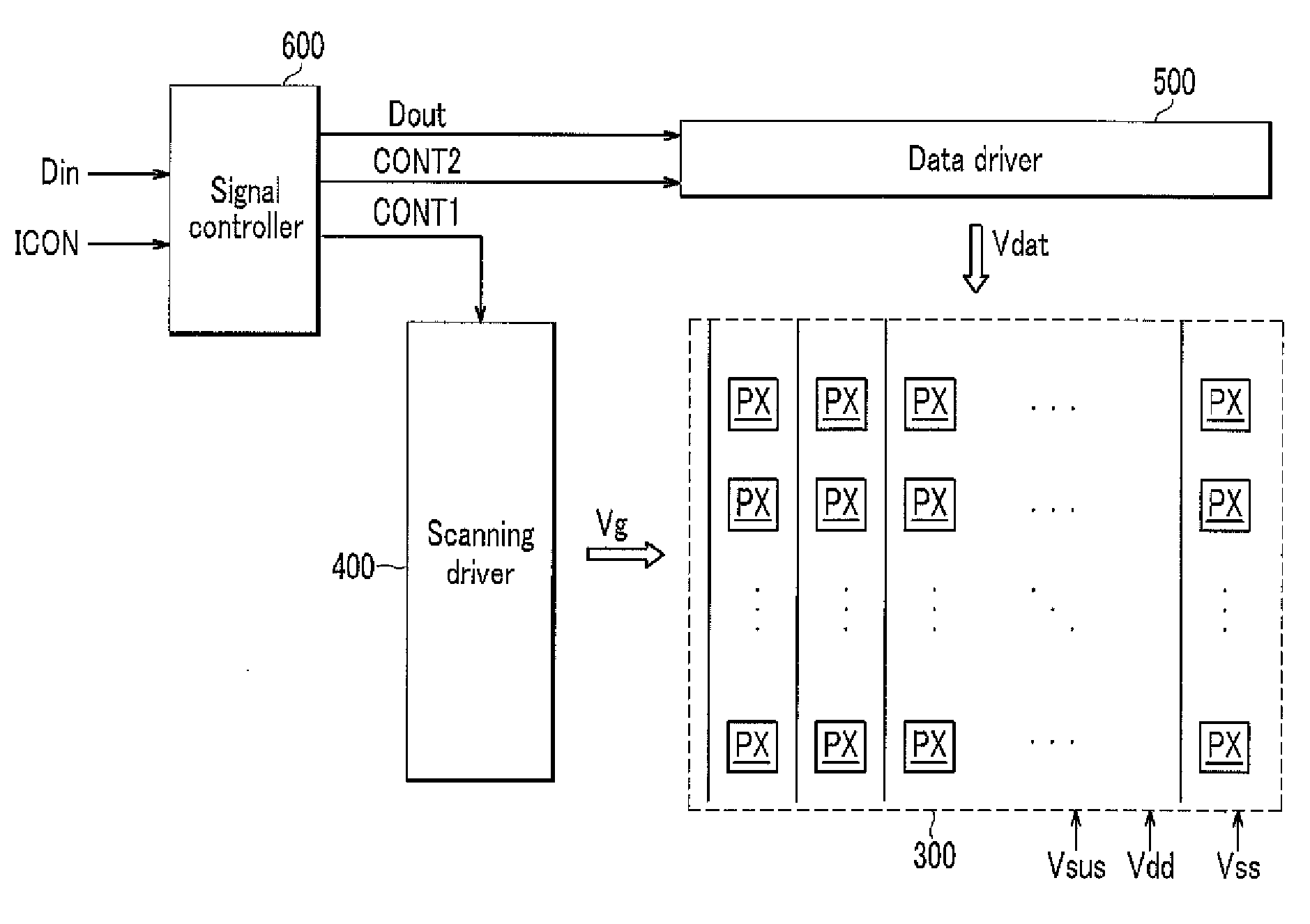
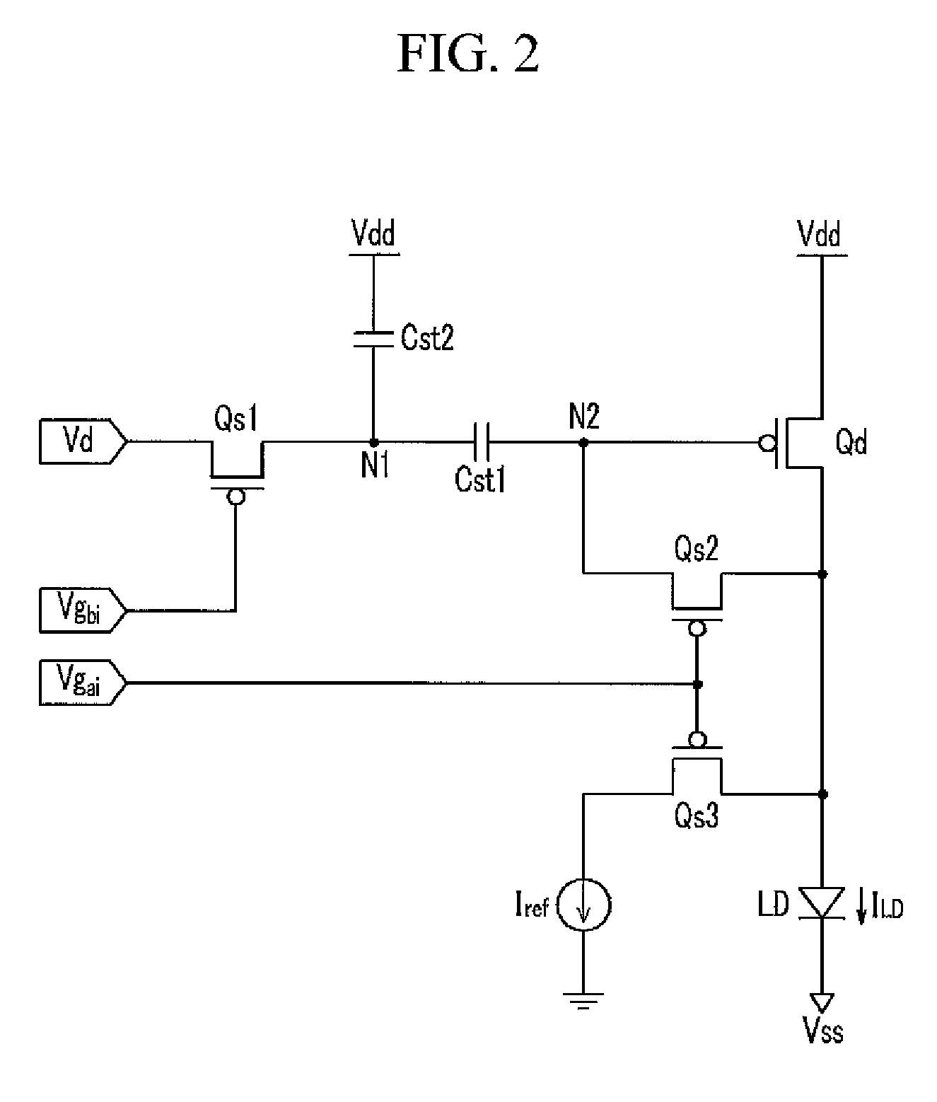
[0053]FIG. 1 is a block diagram of an organic light emitting device according to an exemplary embodiment of the present invention, and FIG. 2 is an equivalent circuit diagram of one pixel in an organic light emitting device according to an exemplary embodiment of the present invention.

[0054]Referring to FIG. 1, the organic light emitting device includes a display panel 300, a scanning driver 400, a data driver 500, and a sign...


PUM


Abstract

A display device and a method of driving the same, in which the display device includes: a light-emitting element; a first capacitor connected between first and second contact points; a driving transistor that has a control terminal connected to the second contact point, an input terminal connected to a driving voltage, and an output terminal connected to the light-emitting element; a first switching transistor connected between a data voltage or a sustain voltage and the first contact point; a second switching transistor connected between the second contact point and the output terminal of the driving transistor; and a third switching transistor connected between a reference current source and the output terminal of the driving transistor.

Description

CROSS-REFERENCE TO RELATED APPLICATION[0001]This application claims priority to and the benefit of Korean Patent Application No. 10-2008-0121288 filed in the Korean Intellectual Property Office on Dec. 2, 2008, the entire contents of which are incorporated herein by reference.BACKGROUND[0002](a) Technical Field[0003]The present disclosure relates to a display device and a method of driving the same. More particularly, the present disclosure relates to an organic light emitting device and a method of driving the same.[0004](b) Discussion of Related Art[0005]A pixel of an organic light emitting device includes an organic light emitting element, along with a thin film transistor (TFT) and a capacitor that drive the light emitting element.[0006]The TFT is classified as a polysilicon TFT or an amorphous silicon TFT, according to the kind of active layer.[0007]Because amorphous silicon is deposited at a low temperature and forms a thin film, the amorphous silicon is generally used for a s...

Claims


Application Information

Patent Timeline
IPC IPC(8): G06F3/038G09G3/32
CPCG09G3/3233G09G2300/0819G09G2320/043G09G2300/0861G09G2320/0223G09G2300/0852H01L21/02579H01L31/182
Inventor HAN, SANG-MYEONCHOI, JAE BEOMKIM, BONG-JULEE, KWON-HYUNGEOM, JI-HYEJUN, SANG-HYANHWANG, HYUN-BEEN
Owner SAMSUNG DISPLAY CO LTD
Why Eureka
Try Eureka