Sensor and method for the manufacture thereof

Active Publication Date: 2010-06-10
ROBERT BOSCH GMBH
View PDF1 Cites 8 Cited by
  • Summary
  • Abstract
  • Description
  • Claims
  • Application Information

AI Technical Summary

Benefits of technology

[0008]The present invention implements a diode structure in a polycrystalline semiconductor material, in particular polysilicon. It is thereby possible, in particula

Problems solved by technology

Manufacture is, however, quite complex, especially including implementati

Method used


Image

  • Sensor and method for the manufacture thereof
  • Sensor and method for the manufacture thereof
  • Sensor and method for the manufacture thereof

Examples


Embodiment Construction

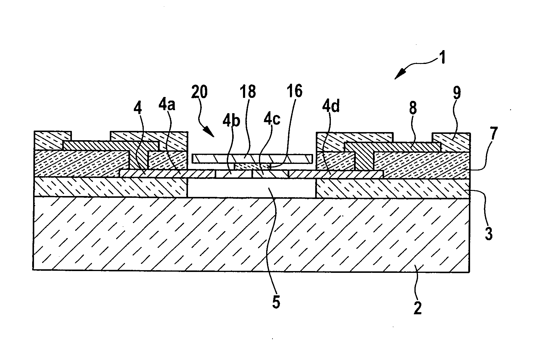
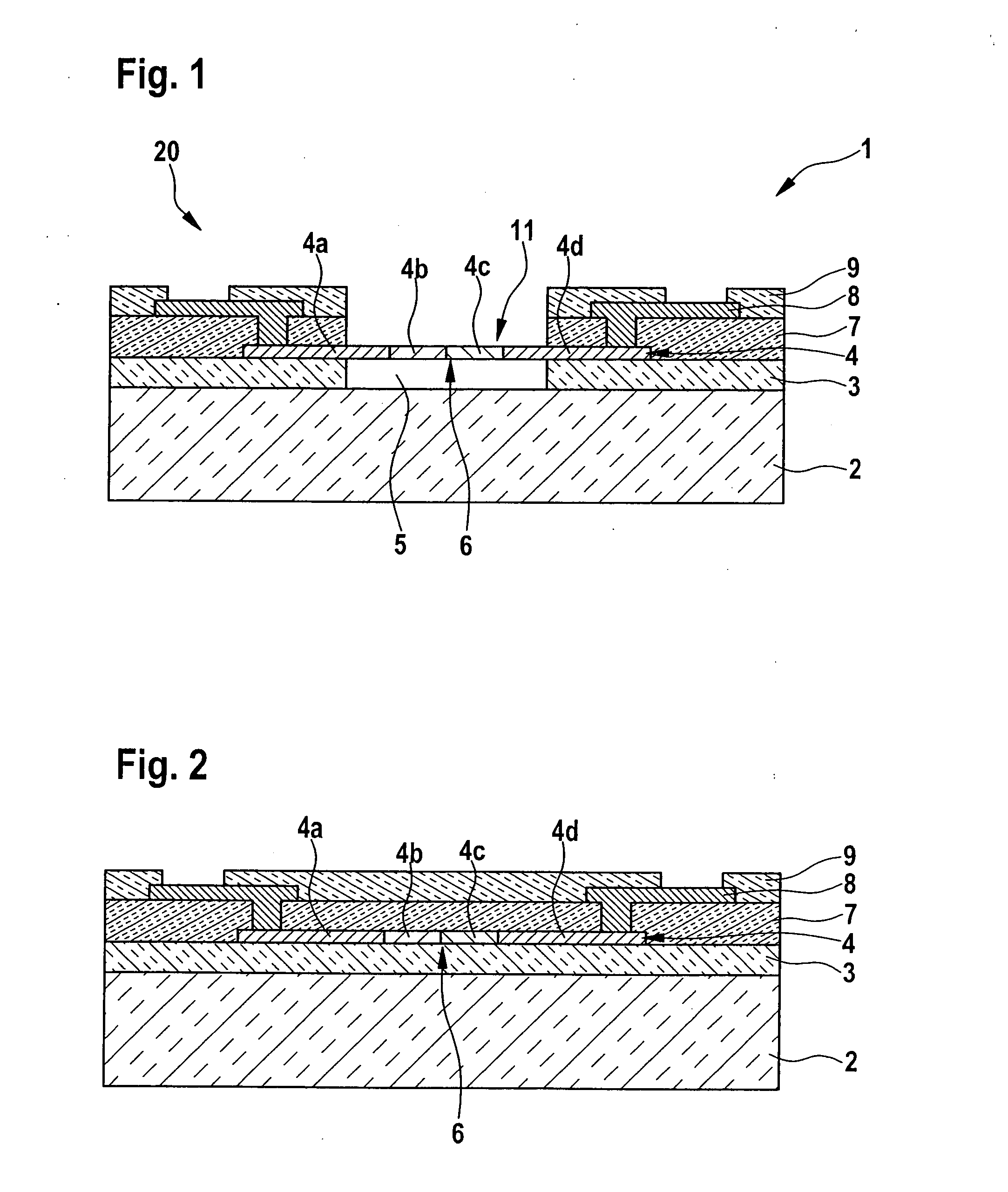
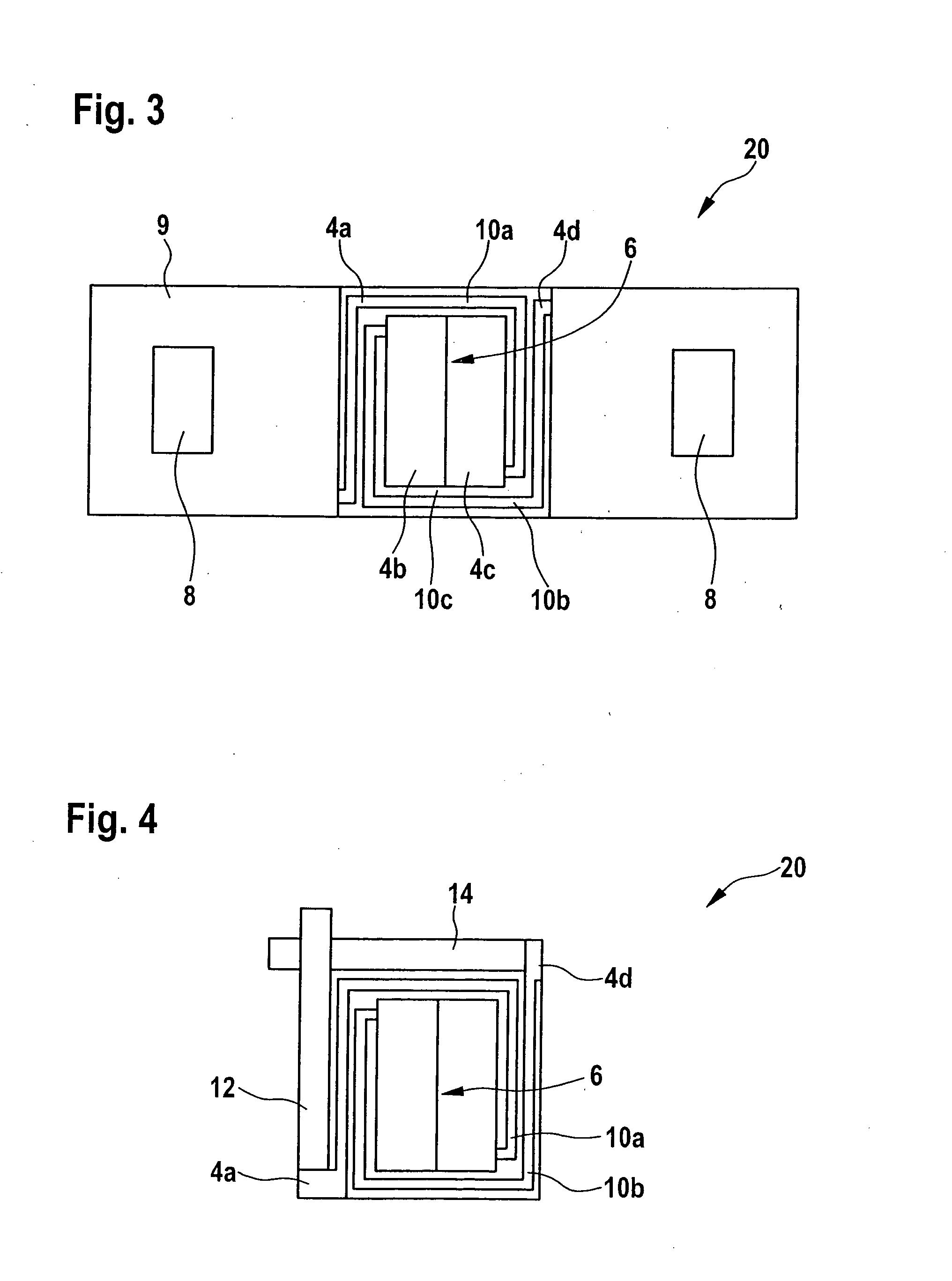
[0024]A sensor 1 has a substrate 2, preferably made of silicon, and has on substrate 2 a patterned layer sequence that has, from bottom to top, firstly a lower insulating layer 3 implemented on substrate 2. Lower insulating layer 3 can be constituted in particular as an oxide layer, preferably as a field oxide layer 3 implemented by oxidation using CMOS process technology, which can e.g. also serve in MOSFETs as a gate oxide layer. Applied onto field oxide layer 3 is a doped polycrystalline semiconductor layer 4 that can be, in particular, a differently doped polysilicon layer 4.

[0025]A cavity 5 is implemented in field oxide layer 3 and beneath polysilicon layer 4. Polysilicon layer 4 thus extends partly above cavity 5. In accordance with the embodiment shown, four regions in polysilicon layer 4 are different doped, namely (laterally adjacent to one another) a p+-doped region 4a, a p-doped region 4b, an n-doped region 4c, and an n+-doped region 4d. The two outer, highly-doped region...


PUM


Abstract

A sensor includes at least one micro-patterned diode pixel that has a diode implemented in, on, or under a diaphragm, and the diaphragm in turn being implemented above a cavity. The diode is contacted via supply leads that are implemented at least in part in, on, or under the diaphragm, and the diode is implemented in a polycrystalline semiconductor layer. The diode is implemented by way of two low-doped diode regions or at least one low-doped diode region. At least parts of the supply leads are implemented by way of highly doped supply lead regions of the shared polycrystalline semiconductor layer.

Description

BACKGROUND OF THE INVENTION[0001]1. Field of the Invention[0002]The present invention relates to a sensor for spatially resolved detection of IR radiation, and also relates to a method for the manufacture thereof.[0003]2. Description of Related Art[0004]Published international patent application document WO 2007 / 147663 A1 describes a sensor of this kind having an array assemblage of diode pixels, each diode pixel having a monocrystalline region beneath a cantilevered diaphragm. A pn diode is implemented as a sensitive region in the monocrystalline region. Supply leads of the diodes to combined column and row terminals are provided in or beneath the diaphragm, so that simple addressing and reading of the diode pixels in an array is possible.[0005]Contacting of the p-doped and n-doped regions of each diode pixel is accomplished via metallic supply leads that firstly contact highly doped regions in the monocrystalline regions beneath the diaphragm, by way of which the p- and n-doped re...

Claims


Application Information

Patent Timeline
IPC IPC(8): H01L31/103H01L31/18
CPCG01J5/08H01L27/14649G01J5/20G01J5/0853
Inventor REINMUTH, JOCHENDAVIES, NEILARMBRUSTER, SIMONFEYH, ANDO
Owner ROBERT BOSCH GMBH
Why Eureka
Try Eureka