Display device manufacturing method and apparatus thereof

a manufacturing apparatus and display device technology, applied in the manufacture of electric discharge tubes/lamps, discharge tubes luminescnet screens, instruments, etc., can solve the problems of time-consuming, complicated and time-consuming steps, and the inability to sufficiently enhance the production efficiency of the display device, etc., to achieve the effect of favorable cutting

Inactive Publication Date: 2010-06-10
PANASONIC LIQUID CRYSTAL DISPLAY CO LTD +1
View PDF4 Cites 15 Cited by
  • Summary
  • Abstract
  • Description
  • Claims
  • Application Information

AI Technical Summary

Benefits of technology

[0023]According to the above-mentioned inventions, it is possible to provide the manufacturing method of a display device, the manufacturing apparatus of a display device which can favorably cut the display panel having the structure where the resin layer is sandwiched between the element substrate and the sealing substrate, and the display device manufactured by the manufacturing method.

Problems solved by technology

However, such a method requires a complicated and time-consuming step where the sealing material is applied to the substrate such that the sealing material surrounds the peripheries of the plurality of display parts individually, and the resin is filled in the inside of the respective display parts surrounded by the sealing material.
Accordingly, it is impossible to sufficiently enhance the production efficiency of the display device.

Method used


Image

  • Display device manufacturing method and apparatus thereof
  • Display device manufacturing method and apparatus thereof
  • Display device manufacturing method and apparatus thereof

Examples


Embodiment Construction

[0027]Hereinafter, a first preferred embodiment of the present invention is explained in conjunction with drawings.

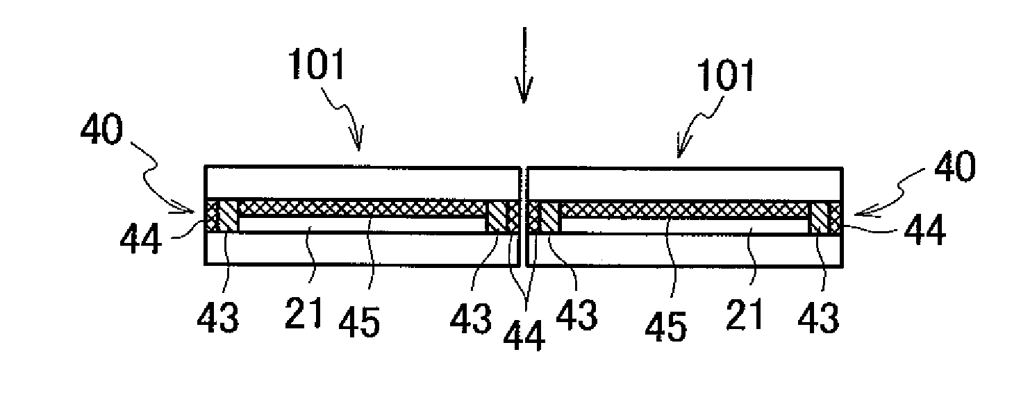
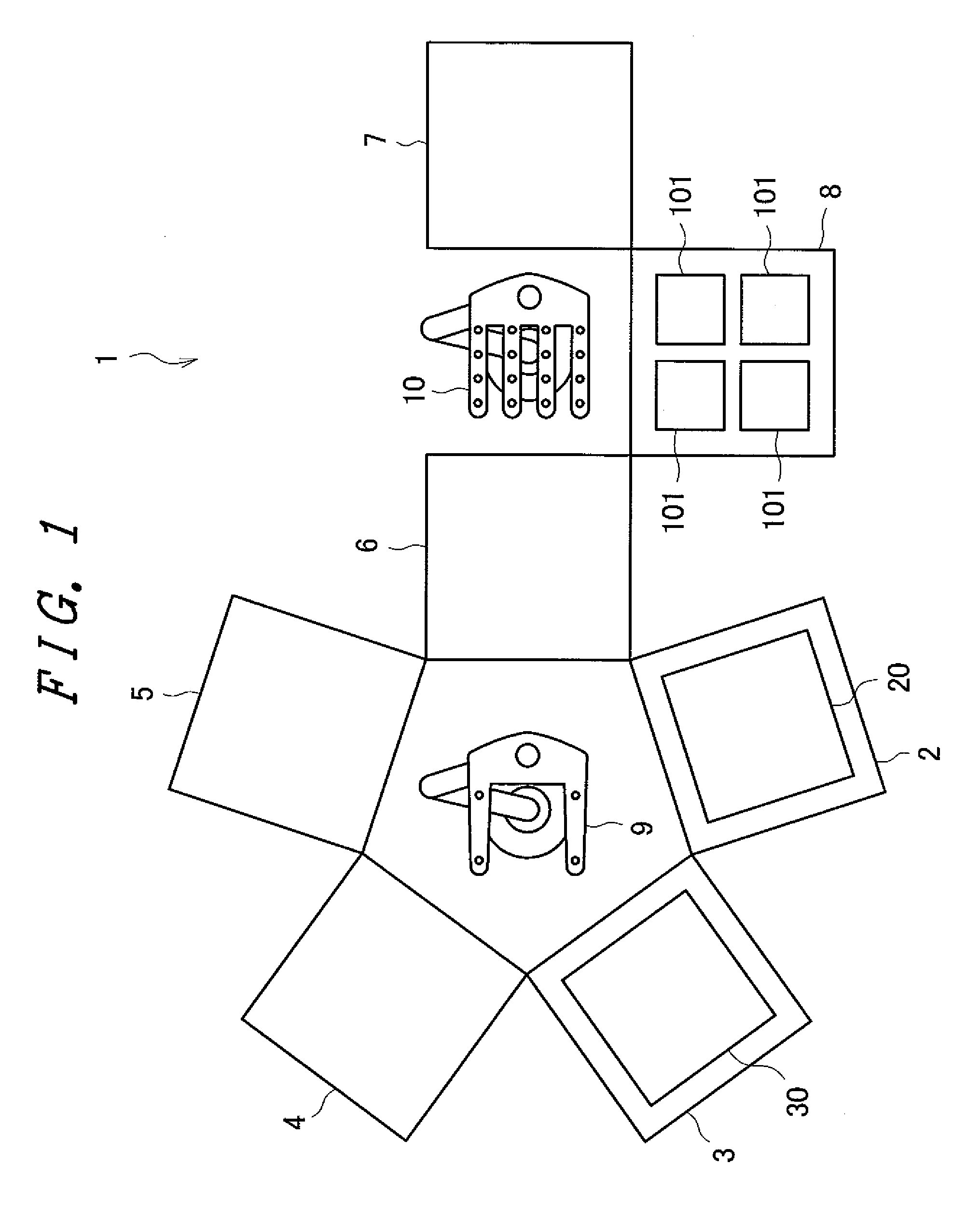
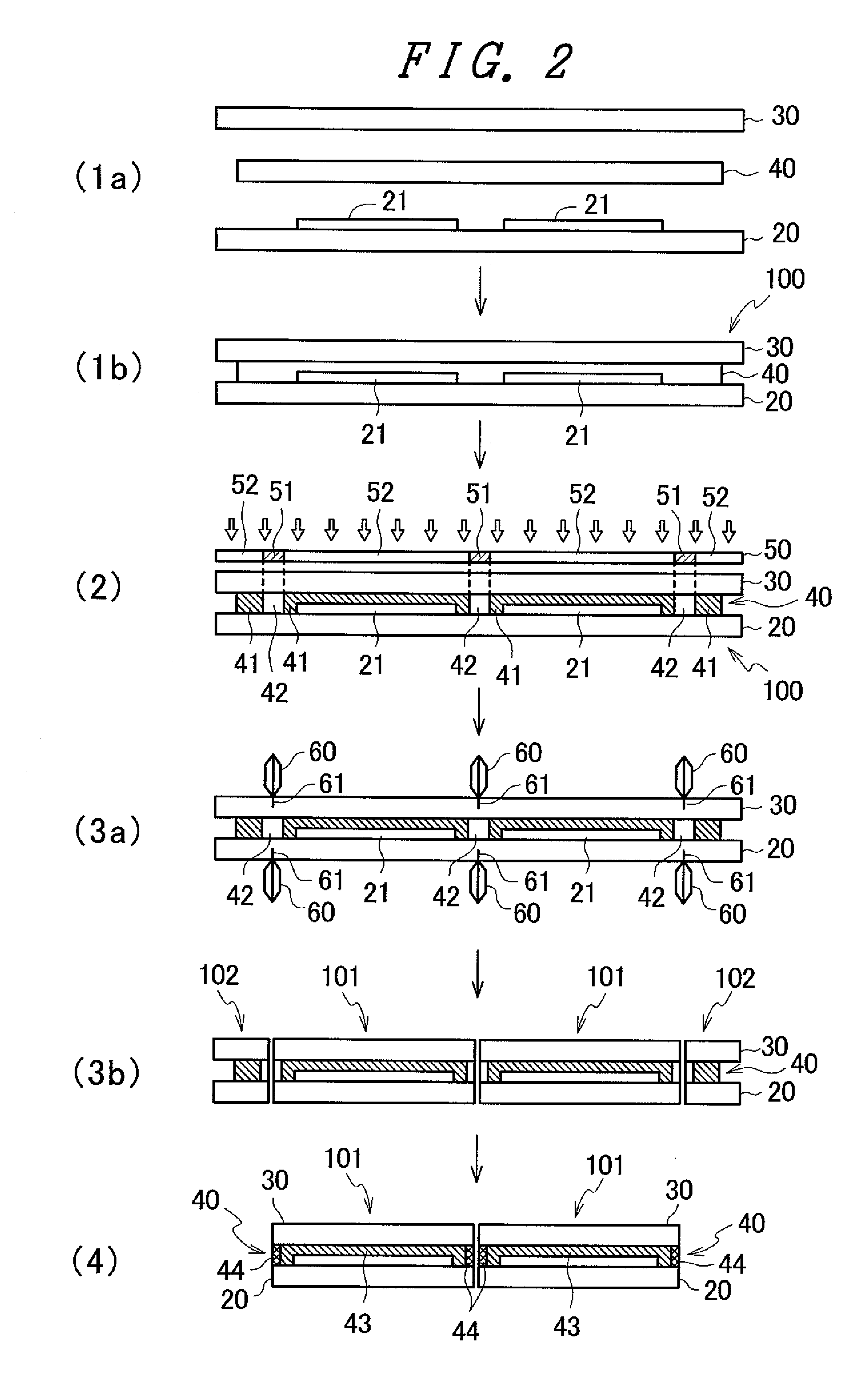
[0028]FIG. 1 is a schematic view of a manufacturing apparatus 1 of a display device 101 according to this embodiment. FIG. 1 shows a state of the manufacturing apparatus 1 as viewed in a plan view. The manufacturing apparatus 1 is constituted of an element substrate receiving portion 2, a sealing substrate receiving portion 3, an adhesion device 4, a radiation device 5, a separation device 6, a heating device 7, a delivery portion 8, a receiving-side conveying device 9 and a delivery-side conveying device 10.

[0029]The element substrate receiving portion 2 is a buffer which receives and stocks an element substrate 20 on which a plurality of light emitting elements are formed, and the sealing substrate receiving portion 3 is a buffer which receives and stocks a sealing substrate 30. The element substrate 20 and the sealing substrate 30 are conveyed from a preceding step u...


PUM


Abstract

The present invention provides a manufacturing method of a display device which can favorably cut a display panel having the structure where a resin layer is sandwiched between an element substrate and a sealing substrate. The manufacturing method of a display device includes the steps of: forming a display panel by sandwiching a resin which is hardened by any one of electromagnetic waves, radioactive rays and electron beams and heat between an element substrate having a display region in which a plurality of light emitting elements are formed and a sealing substrate in such a manner that the resin covers the display region; radiating at least one of electromagnetic waves, radioactive rays and electron beams to the display panel thus hardening first portions of the resin and leaving second portions of the resin in a state softer than the first portions; separating the display panel at positions corresponding to the second portions; and heating the separated display panel thus further hardening the resin.

Description

CROSS-REFERENCE TO RELATED APPLICATIONS[0001]The present application claims priority from Japanese Application JP 2008-309527 filed on Dec. 4, 2008, the content of which is hereby incorporated by reference into this application.BACKGROUND OF THE INVENTION[0002]1. Field of the Invention[0003]The present invention relates to a manufacturing method of a display device, a manufacturing apparatus of a display device, and a display device, and more particularly to a manufacturing method of a display device having a display region in which a plurality of light emitting elements are formed, a manufacturing apparatus of a display device, and a display device.[0004]2. Background Art[0005]Recently, there has been proposed a display device which displays various kinds of information by integrating a large number of light emitting elements on a substrate. As a typical example of such a display device, an organic electroluminescence display (OLED) which makes use of emission of light by electrolu...

Claims


Application Information

Patent Timeline
Patent Type & Authority Applications(United States)
IPC IPC(8): H01J1/62H01J9/26H01J9/46
CPCG02F1/133351G02F1/1339H05B33/10H01L51/56H01L2251/566H01L51/5237H10K50/8426H10K71/00H10K71/851
Inventor KASE, SATORUISHII, YOSHINORIMATSUZAKI, EIJI
Owner PANASONIC LIQUID CRYSTAL DISPLAY CO LTD
Why Eureka
Try Eureka