METHOD OF GROWING PURE Ge THIN FILM WITH LOW THREADING DISLOCATION DENSITY

a thin film, low-density technology, applied in the direction of single crystal growth, polycrystalline material growth, chemistry apparatus and processes, etc., can solve the problems of deterioration of device characteristics, time-consuming process taking almost 4 hours, and leakage curren

Inactive Publication Date: 2010-06-10
ELECTRONICS & TELECOMM RES INST
View PDF10 Cites 6 Cited by
  • Summary
  • Abstract
  • Description
  • Claims
  • Application Information

AI Technical Summary

Benefits of technology

[0014]One aspect of the present invention provides a method of growing a germanium (Ge) single crystal thin film with low threading dislocation density using reduced pressure chemical vapor deposition (RPCVD), including: growing a Ge thin film on a silicon (Si) substrate at a low temperature; performing real-time annealing for a short period of time; and growing the annealed Ge thin film at a high temperature.
[0015]Another aspect of the present invention provides a method of growing a Ge single crystal thin film with low threading dislocation density using RPCVD, including: growing a Ge thin film on a Si substrate at a low temperature; performing real-time annealing for a short period of time; growing a Si—Ge thin layer after real-time annealing; and growing the annealed Ge thin film at a high temperature on the Si—Ge thin layer.

Problems solved by technology

The threading dislocation propagated to the surface may cause defects of a thin film to be formed thereon, deteriorating device's characteristics or causing leakage current.
However, since this method requires high-priced UHVCVD equipment, and annealing cannot be performed in UHVCVD, rapid thermal processing (RTP) should be added, which is a time-consuming process taking almost 4 hours.
Further, due to interdiffusion between Si and Ge caused by high-temperature annealing, a Si—Ge layer is formed at an interface, affecting a change in band-gap and the device's characteristics.
The misfit dislocation may be a cause of deterioration of the device's characteristics during the fabrication of the device.

Method used


Image

  • METHOD OF GROWING PURE Ge THIN FILM WITH LOW THREADING DISLOCATION DENSITY
  • METHOD OF GROWING PURE Ge THIN FILM WITH LOW THREADING DISLOCATION DENSITY
  • METHOD OF GROWING PURE Ge THIN FILM WITH LOW THREADING DISLOCATION DENSITY

Examples


example 1

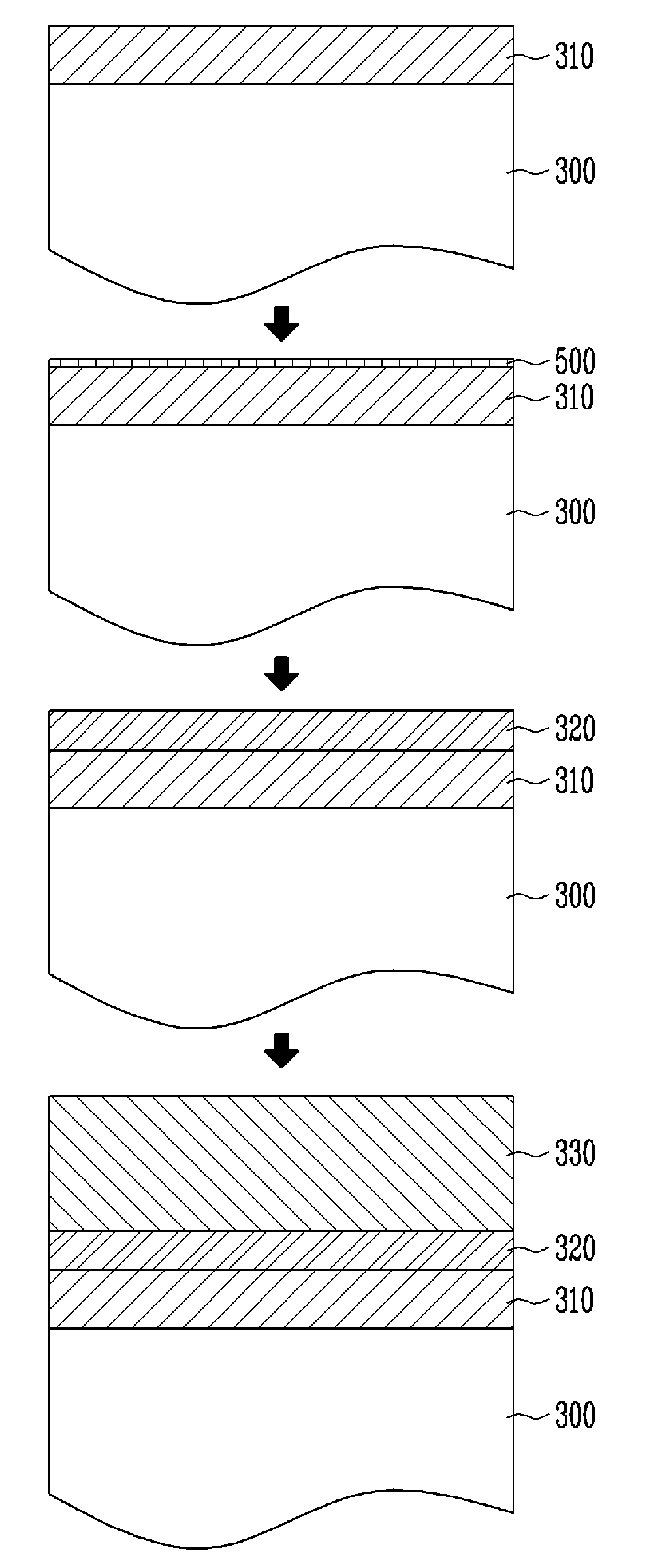
[0044]In RPCVD, GeH4 diluted to 20 vol % with hydrogen was injected to a silicon substrate at a flow rate of 200 sccm under the conditions of 400° C. 15 and 30 torr, and hydrogen gas was injected at a flow rate of 20 slm to grow a Ge thin film to a thickness of 100 nm. Subsequently, in RPCVD, the injection of the GeH4 gas was stopped, a temperature was increased to 875° C. at a rate of 200° C. per minute, and annealing was performed for 10 minutes. After annealing, the temperature was decreased at the same rate at which it was increased, 200° C. per minute, and the GeH4 gas was injected at a flow rate of 40 sccm under the conditions of 700° C. and 80 torr to grow the Ge thin film to a thickness of 1400 nm.

experimental example

[0045]Analysis of Ge Concentration after Annealing

[0046]After real-time annealing the Ge thin film having a thickness of 100 nm grown at a low temperature according to Example 1, the Ge concentration was obtained through SIMS analysis, and the result is shown in FIG. 4.

[0047]As shown in FIG. 4, the low-temperature Ge thin film grown over the silicon substrate was changed into a Si—Ge thin film (Si0.16Ge0.84) having a Ge content of 84 at % on its surface by gradually increasing the Ge content through annealing.

[0048]Analysis of Ge Concentration of Ge Single Crystal Thin Film

[0049]The Ge concentrations of the Ge single crystal thin film formed using RPCVD according to Example 1 and the conventional Ge thin film (shown in FIG. 1) formed using UHVCVD were obtained through SIMS analysis, and the result is shown in FIG. 5. As shown in FIG. 5, the conventional Ge thin film was changed into a Si—Ge layer whose thickness was ⅓ of the overall thickness. The Si—Ge layer was formed by interdiff...


PUM

PropertyMeasurementUnit
pressureaaaaaaaaaa
temperatureaaaaaaaaaa
thicknessaaaaaaaaaa

Abstract

Provided is a method of growing a pure germanium (Ge) thin film with low threading dislocation density using reduced pressure chemical vapor deposition (RPCVD), which includes growing a Ge thin film on a silicon (Si) substrate at a low temperature, performing real-time annealing for a short period of time, and growing the annealed Ge thin film at a high temperature. The grown Ge single crystal thin film can overcome conventional problems of generation of a Si—Ge layer due to Si diffusion, and propagation of misfit dislocation to a high-temperature Ge thin film.

Description

CROSS-REFERENCE TO RELATED APPLICATION[0001]This application claims priority to and the benefit of Korean Patent Application No. 10-2008-0123326, filed Dec. 5, 2008, the disclosure of which is incorporated herein by reference in its entirety.BACKGROUND[0002]1. Field of the Invention[0003]The present invention relates to a pure germanium (Ge) single crystal layer, which is grown on a silicon substrate, and more particularly, to a method of forming a stress relaxed Ge single crystal thin film, low threading dislocation density and good surface roughness using reduced pressure chemical vapor deposition (RPCVD).[0004]2. Discussion of Related Art[0005]Development of novel devices using heterojunctions of silicon (Si) and silicon-germanium (Si—Ge) or germanium (Ge) has been conducted for several decades. These devices generally utilize a difference in band-gap energy between Si and Ge, or high-mobility characteristics generated due to stress applied according to a difference of lattice co...

Claims


Application Information

Patent Timeline
Patent Type & Authority Applications(United States)
IPC IPC(8): H01L21/205
CPCC30B25/02C30B29/08H01L21/0262H01L21/02532H01L21/02381H01L21/205H01L21/20H01L21/324
Inventor KIM, SANG HOONSUH, DONG WOOJOO, JI HOKIM, GYUNG OCKKIM, HYUN TAK
Owner ELECTRONICS & TELECOMM RES INST
Why Eureka
Try Eureka