
System And Method For Maintaining Cache Coherency Across A Serial Interface Bus

a serial interface and cache technology, applied in computing, memory address/allocation/relocation, instruments, etc., can solve the problems of multiple cpus in conventional systems that cannot read and cache data, data cannot be stored in an intervening cache, and may have side effects expected by computing systems and required for normal operations. the effect of processing speed

Active Publication Date: 2010-06-10
NVIDIA CORP
View PDF6 Cites 6 Cited by
  • Summary
  • Abstract
  • Description
  • Claims
  • Application Information

AI Technical Summary

Benefits of technology

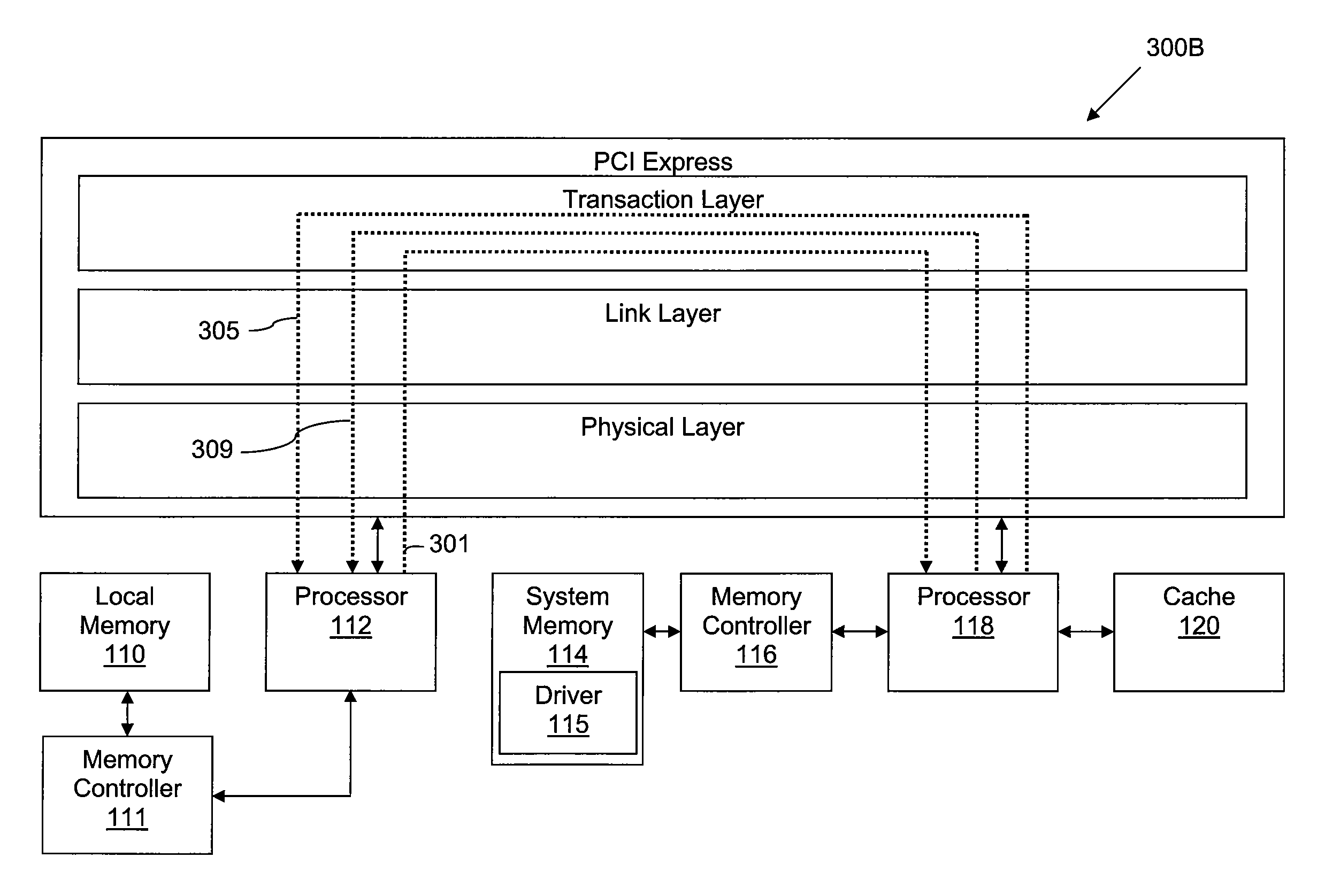
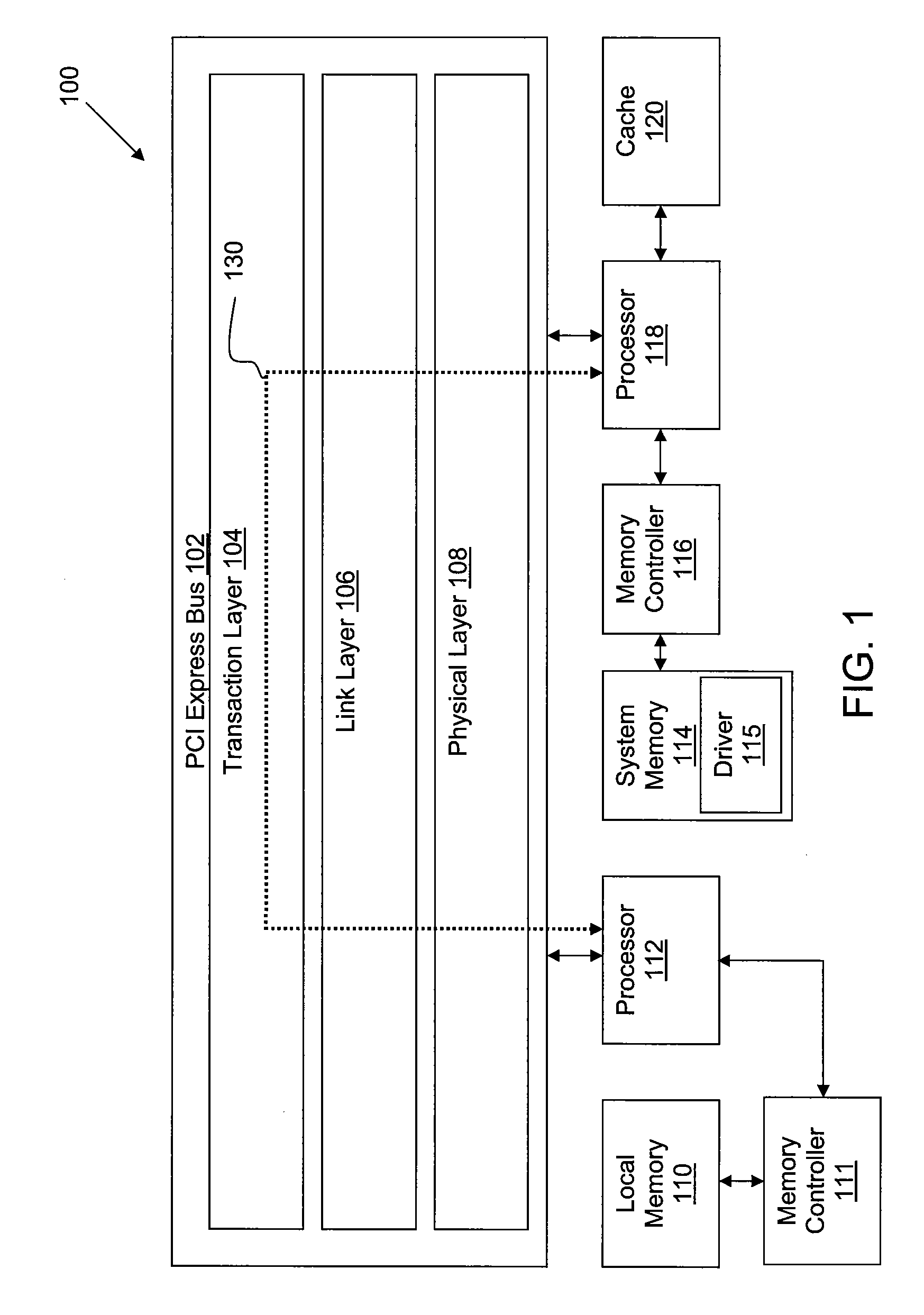
[0010]One embodiment of the invention sets forth a method for executing a processing operation using data stored in a data cache. The method comprises generating a snoop request configured to determine whether first data stored in a local memory coupled to a first processor is coherent relative to second data stored in a data cache coupled to a second processor, the snoop request including destination information that identifies the data cache on a serial interface bus, and a cache line address identifying where in the data cache the second data is located; causing the snoop request to be transmitted over the serial interface bus to the second processor based on the destination information that identifies the data cache; extracting the cache line address from the snoop request; determining whether the second data stored in the data cache at the cache line address is coherent relative to the first data stored in the local memory; generating a complete (CPL) message that includes destination information that identifies the local memory on the serial interface bus, and completion information indicating that the first data is coherent relative to the second data; causing the CPL message to be transmitted over the serial interface bus to the first processor based on the destination information that identifies the local memory; and causing the processing operation to be executed on the first processor using the first data stored in the local memory.
[0011]Advantageously, data transmitted across the PCIe bus may be marked as “cacheable,” removing the need for processors that receive this data to serialize the execution of program instructions. Thus, processor speed is improved when performing operations with data received over the PCIe bus relative to prior art approaches.

Problems solved by technology

However, multiple CPUs in conventional systems cannot read and cache data across PCIe because there currently does not exist a way to maintain cache coherency across PCIe.
In such a case, referencing this data may have side effects that are expected by the computing system and required for normal operations.
Thus, this data cannot be stored in an intervening cache without risking unpredictable operation of the computing system.
One problem with the aforementioned configuration is that when a processor reads data that is marked UC or WC, that data cannot be cached by the processor.
For example, if the processor executes multiple processing operations using the same data that was marked UC or WC, then the processor would be required to read the data from an external (non-cache) memory unit multiple times, thus introducing significant latencies.
Another problem is that when a processor executes instructions using data that is marked UC, the processor serializes the execution of those instructions, which reduces the efficiency of the processor.
This data, therefore, cannot be cached, which introduces additional latencies.
However, this solution greatly limits the possible configurations of the computing system.

Method used


Image

  • System And Method For Maintaining Cache Coherency Across A Serial Interface Bus
  • System And Method For Maintaining Cache Coherency Across A Serial Interface Bus
  • System And Method For Maintaining Cache Coherency Across A Serial Interface Bus

Examples


first embodiment

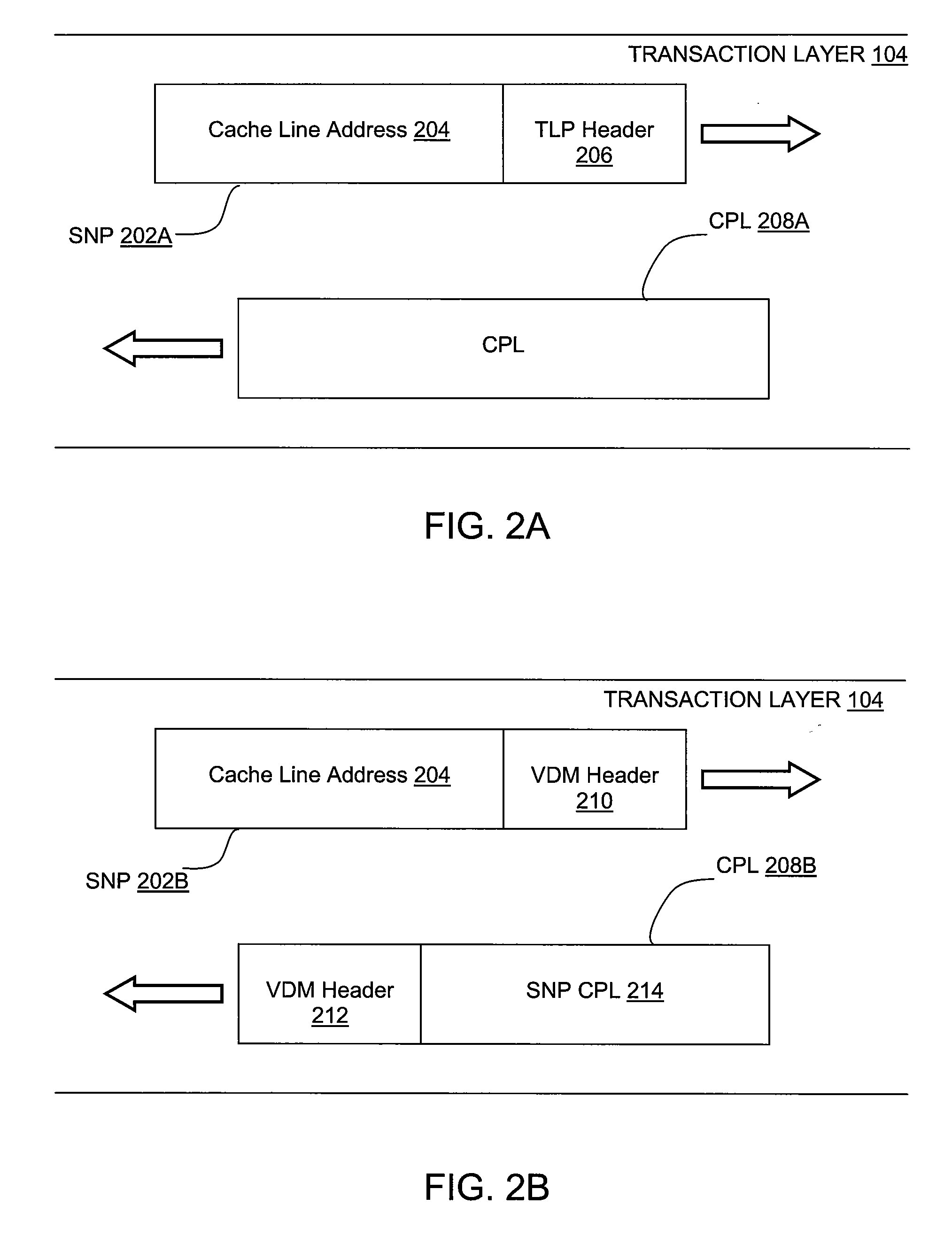
[0028]FIG. 2A is a conceptual diagram illustrating packets associated with a SNP transaction, according to one embodiment of the invention. As shown, FIG. 2A illustrates a SNP request 202A and a CPL message 208A travelling through the transaction layer 104. In one embodiment, the SNP 202A and the CPL message 208A do not travel through the transaction layer simultaneously, as described in greater detail herein. The SNP request 202A includes a cache line address 204 and a transaction layer packet (TLP) header 206. The cache line address 204 specifies the address of the cache line to be examined. The TLP header 206 identifies the message as a SNP request 202A to the recipient of the message.

[0029]The SNP request 202A may be added to the PCIe standard protocol as a “non-posted transaction.” When a first PCIe endpoint transmits a non-posted transaction to a second PCIe endpoint, the first PCIe endpoint expects a CPL message in response. Thus, when the processor 112 transmits the SNP requ...

second embodiment

[0031]FIG. 2B is a conceptual diagram illustrating packets associated with a SNP transaction, according to one embodiment of the invention. As shown, FIG. 2B illustrates a SNP request 202B and a CPL message 208B travelling through the transaction layer 104. In one embodiment, the SNP request 202B and the CPL message 208B do not travel through the transaction layer 104 simultaneously. SNP request 202B includes a cache line address 204 and a vendor-defined message (VDM) header 210. The CPL message 208B includes a VDM header 210 and a SNP CPL 214. The SNP request 202B and the CPL message 208B are both VDMs and are not included in the PCIe standard protocol. The processor 112 uses the SNP request 202A and the SNP request 208B in a similar fashion to initiate a SNP transaction. The processor 118 uses the CPL 208A message and the CPL 208B message in a similar fashion to indicate that the SNP transaction is complete.

[0032]When the processor 112 transmits the SNP request 202B to the process...

third embodiment

[0059]At step 506, the processor 118 adds a completion status to the CPL message. In one embodiment, the completion status is a read completion notification. In an alternative embodiment, the completion status indicates that no action was taken. In yet a third embodiment, the completion status is blank. At step 608, the processor 118 adds destination information to the packet. The destination information identifies the processor 112 as the intended recipient of the CPL message. The PCIe bus includes logic that routes the CPL message to the processor 112 according to the destination information. When the processor 112 receives the CPL message, the SNP transaction is complete, and the local memory 110 is coherent with the cache 120.

[0060]In sum, embodiments of the invention provide a technique to perform a “snoop” (SNP) transaction on the PCIe bus. A SNP transaction is implemented using a SNP request and a “complete” CPL message. When a first processor stores data in a local memory un...


PUM


Abstract

A method for executing processing operations using data stored in a memory. The method includes generating a snoop request configured to determine whether first data stored in a local memory is coherent relative to second data stored in a data cache, the snoop request including destination information that identifies the data cache on a bus, and a cache line address identifying where in the data cache the second data is located. The method further includes causing the snoop request to be transmitted over the bus to the second processor, extracting the cache line address from the snoop request, determining whether the second data is coherent, generating a complete message that includes completion information indicating that the first data is coherent with the second data, and causing the complete message to be transmitted over the bus to the first processor.

Description

BACKGROUND OF THE INVENTION[0001]1. Field of the Invention[0002]The present invention relates generally to the field of distributed computing and more specifically to a system and method for maintaining cache coherency across a serial interface bus, such as PCI Express (PCIe).[0003]2. Description of the Related Art[0004]In conventional computing systems, a processor reads data from an external memory unit and stores a copy of the data in a low-latency cache memory unit (cache) for later use. The processor may then read the copy of the data from the cache instead of reading the data from the external memory unit when executing operations using the data. Since data accesses between the processor and the external memory unit have a higher latency than data accesses between the processor and the cache, retrieving data from the cache allows the processor to execute instructions more quickly, and, ultimately, increases the performance of the processor. Caches are usually implemented as st...

Claims


Application Information

Patent Timeline
Patent Type & Authority Applications(United States)
IPC IPC(8): G06F12/08
CPCG06F12/0831G06F9/06G06F13/14G06F13/38
Inventor LANGENDORF, BRIAN KEITHGLASCO, DAVID B.COX, MICHAEL BRIANALBEN, JONAH M.
Owner NVIDIA CORP
Learn More