Standard Cell Architecture and Methods with Variable Design Rules

a technology of design rules and standard cells, applied in the direction of semiconductor devices, semiconductor/solid-state device details, electrical devices, etc., can solve the problem of restricted design rules for standard cells

Inactive Publication Date: 2010-06-24
TAIWAN SEMICON MFG CO LTD
View PDF6 Cites 84 Cited by
  • Summary
  • Abstract
  • Description
  • Claims
  • Application Information

AI Technical Summary

Benefits of technology

[0025]These and other problems are generally solved or circumvented, and technical advantages are generally achieved, by embodiments of the present invention, which provides a restricted design rule with variable layer to cell boundary spacing distance rule

Problems solved by technology

The standard cells are subject

Method used


Image

  • Standard Cell Architecture and Methods with Variable Design Rules
  • Standard Cell Architecture and Methods with Variable Design Rules
  • Standard Cell Architecture and Methods with Variable Design Rules

Examples


Embodiment Construction

[0042]The making and using of the presently preferred embodiments are discussed in detail below. It should be appreciated, however, that the present invention provides many applicable inventive concepts that can be embodied in a wide variety of specific contexts. The specific embodiments discussed are merely illustrative of specific ways to make and use the invention, and do not limit the scope of the invention.

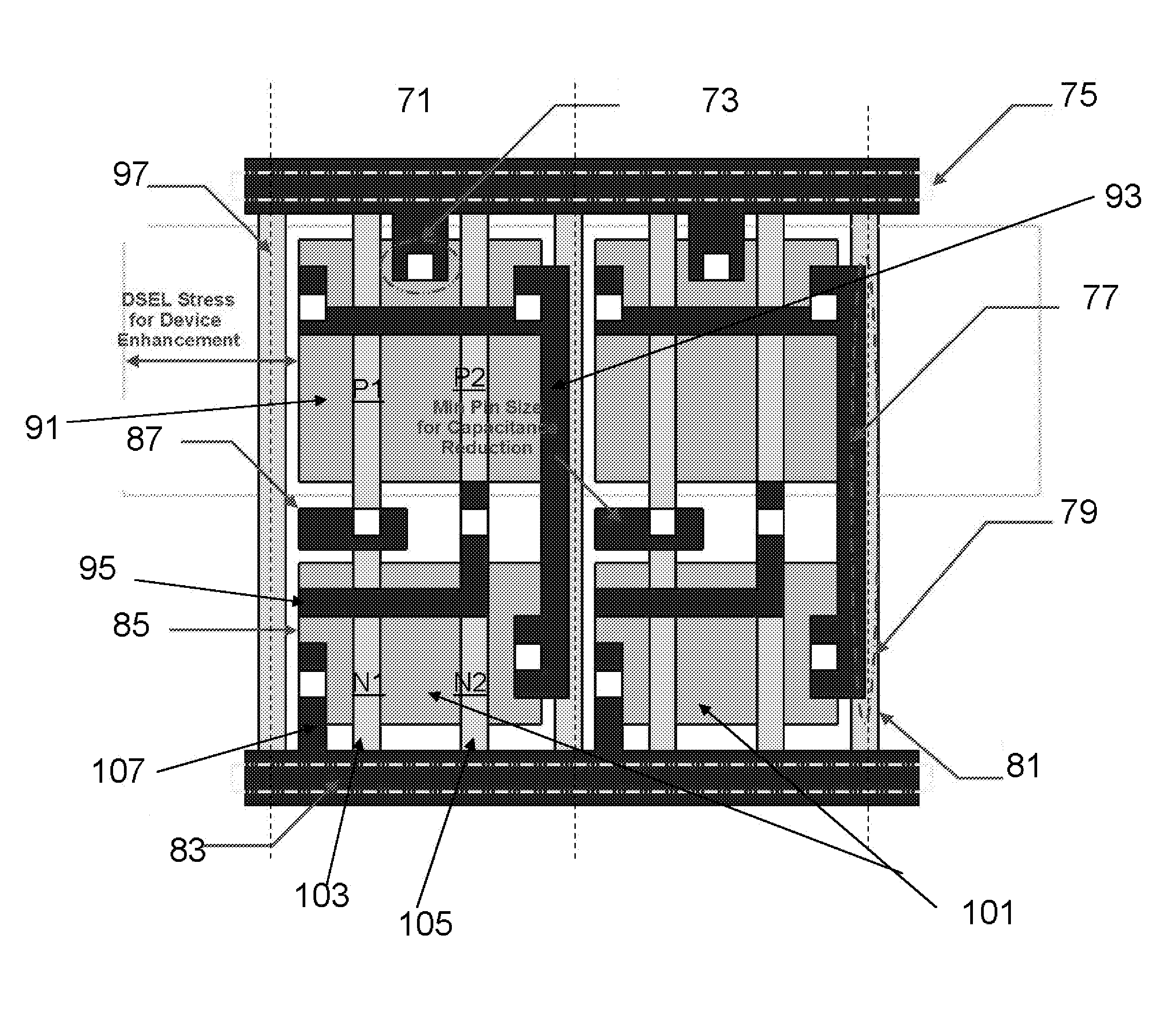
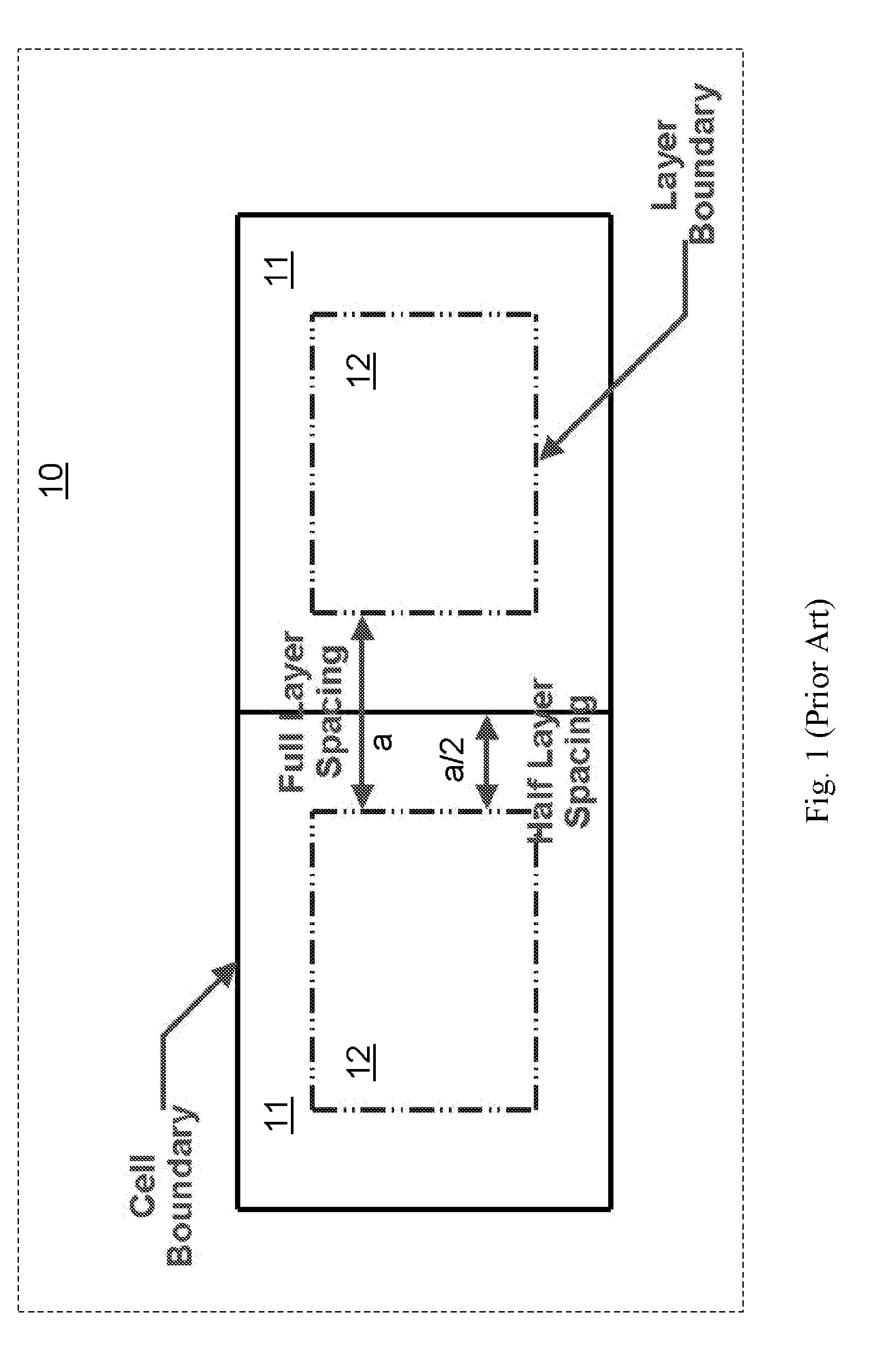
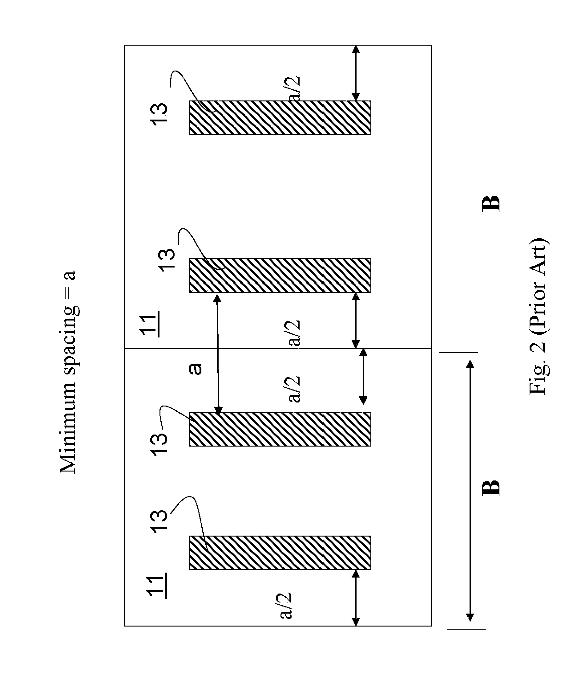
[0043]FIG. 5 depicts in a simple plan view a portion of an integrated circuit. For a non limiting example, the integrated circuit may be an ASIC 50 with two example standard cells 55 and 59 illustrated. This non-limiting example is used to depict the spacing rules of the exemplary embodiment. In FIG. 5, two standard cells 55 and 59 are shown placed adjacent one another. Cell 55 has a layer spacing boundary, for example metal 1 or another layer, bounding an area where the layer may be placed 57. Cell 59 has a layer spacing boundary bounding an area where the same layer may be ...


PUM


Abstract

Structures and methods for standard cell layouts having variable rules for spacing of layers to cell boundaries are disclosed. In one embodiment, a first standard cell layout is provided with a conductive layer having at least two portions spaced apart by a minimum spacing distance, the conductive layer having at least one portion spaced from a cell boundary by a first spacing distance of less than half of the minimum spacing distance; a second standard cell disposed adjacent the first standard cell with at least one second portion of the conductive layer in the second cell disposed adjacent the first portion in the first standard cell and spaced apart from a common cell boundary by a second spacing greater than half of the minimum; wherein the sum of the first and second spacings is at least as great as the minimum spacing. A method for forming standard is disclosed.

Description

TECHNICAL FIELD[0001]The present invention relates to a circuit and methods for providing an improved integrated circuit design and methods using a cell based approach with variable spacing rules to improve the tolerance of a completed integrated circuit to process variations. The invention provides advantages especially at advanced semiconductor process technology nodes having minimum feature sizes of 32 nanometers, and less.BACKGROUND[0002]Presently, system level designers who determine a need for a newly defined integrated circuit, for example to integrate a variety of functions into one chip, often use an application specific integrated circuit (ASIC) or system on a chip (SOC) cell based design. In this approach, a library of known functions is provided, and after the functional design of the device is specified by choosing and connecting these standard functions, and proper operation of the resulting circuit is verified using electronic design automation (EDA) tools, the librar...

Claims


Application Information

Patent Timeline
IPC IPC(8): H01L25/07H01L21/8232
CPCH01L27/0207H01L27/11807H01L2924/0002H01L2924/00
Inventor LAW, OSCAR M.K.JOSHI, MANOJ ACHYUTRAOTHEI, KONG-BENGCHUANG, HARRY
Owner TAIWAN SEMICON MFG CO LTD
Why Eureka
Try Eureka