Gallium nitride compound semiconductor light-emitting device, method of manufacturing the same, and lamp including the same
a technology of compound semiconductors and light-emitting devices, which is applied in the direction of semiconductor/solid-state device manufacturing, semiconductor devices, semiconductor devices, etc., can solve the problems of low light transmittance, low contact resistance, and difficulty in emitted light from the light-emitting device to the outside, so as to prevent an increase in the specific resistance of the p-type semiconductor layer and low specific resistance. , the effect of high emission characteristics
- Summary
- Abstract
- Description
- Claims
- Application Information
AI Technical Summary
Benefits of technology
Problems solved by technology
Method used
Image

Examples
example 1
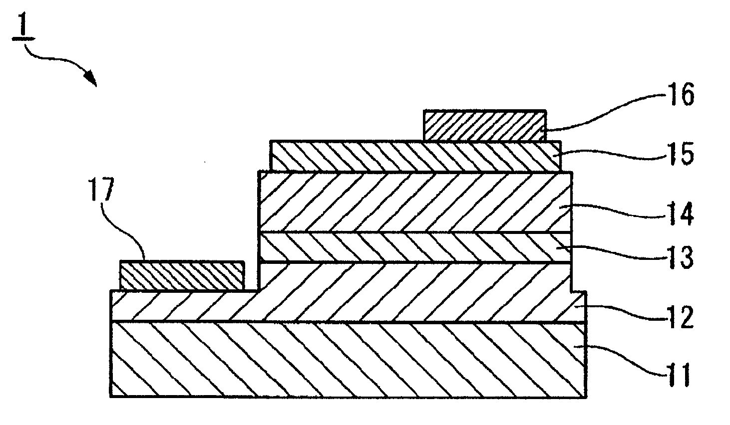
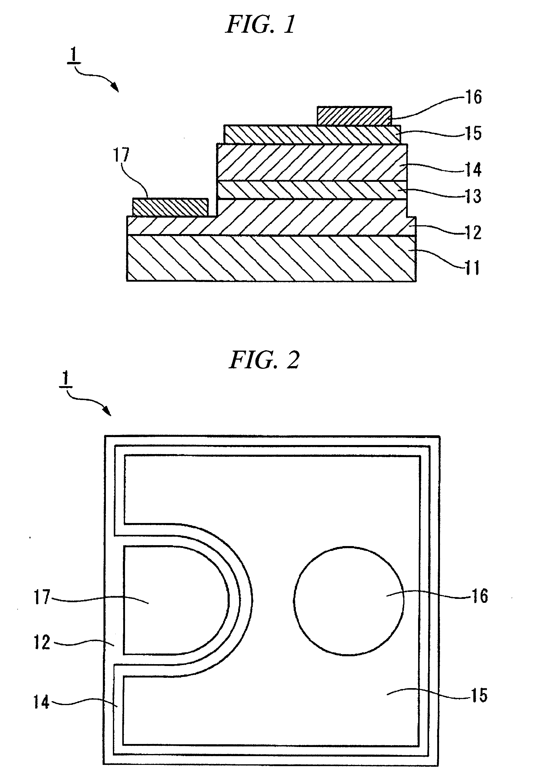
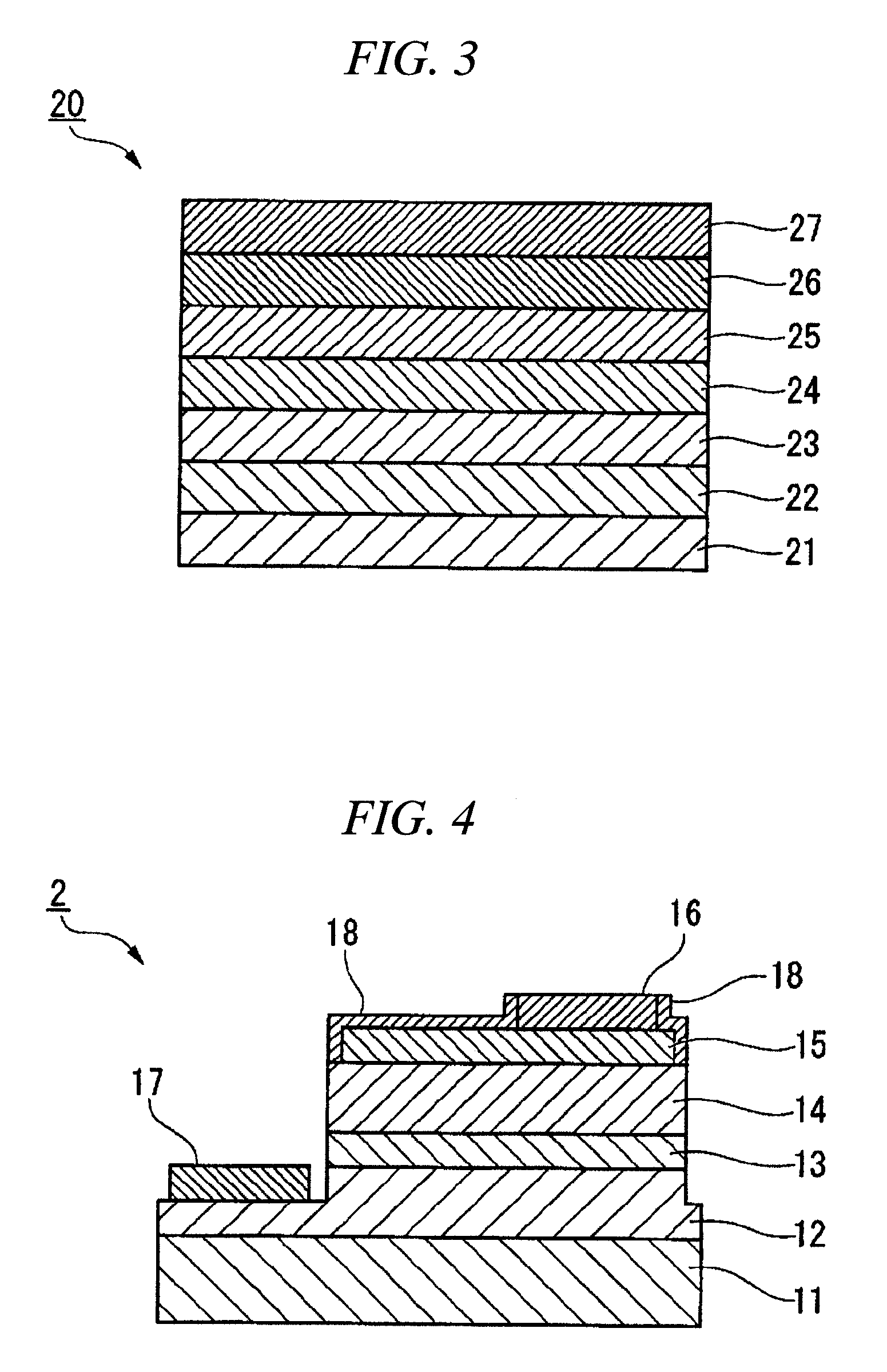
[0120]FIG. 3 is a cross-sectional view schematically illustrating an epitaxial structure used for the gallium nitride compound semiconductor light-emitting device according to Examples of the invention. FIGS. 1 and 2 are respectively a cross-sectional view and a plan view schematically illustrating the gallium nitride compound semiconductor light-emitting device according to the present invention. Next, the gallium nitride compound semiconductor light-emitting device will be described with reference to FIGS. 1 to 3.
(Manufacture of Gallium Nitride Compound Semiconductor Light-Emitting Device)
[0121]The laminated structure of the gallium nitride compound semiconductor 20 shown in FIG. 3 was formed by sequentially laminating, on a c-plane ((0001) crystal surface) sapphire substrate 21, an undoped GaN underlying layer (thickness=2 μm) 22, a Si-doped n-type GaN contact layer (thickness=2 μm, and carrier concentration=1×1019 cm−3) 23, a Si-doped n-type Al0.07Ga0.93N clad layer (thickness=1...
example 2
[0133]A gallium nitride compound semiconductor light-emitting device was manufactured, similar to Example 1, except that wet etching was performed on an ITO film and then the hydrogen annealing process was performed thereon.
[0134]The driving voltage Vf of the light-emitting device according to Example 2 is shown in the graph of FIG. 6.
[0135]The emission power Po of the light-emitting device according to Example 2 was 10 mW.
[0136]In Example 2 in which wet etching is performed on the ITO film and then the hydrogen annealing process is performed thereon, as the temperature is increased, the driving voltage Vf is decreased. However, unlike Example 1, a rapid reduction in the driving voltage Vf at a temperature of about 300° C. does not occur. It is considered that this is because the p-type GaN layer is exposed in a H2 atmosphere and H2 atoms are attracted to the p-type GaN layer. However, the driving voltage Vf is reduced to the same level as that in Example 1 at a temperature of more ...
example 3
[0137]A gallium nitride compound semiconductor light-emitting device was manufactured, similar to Example 1, except that, before the hydrogen annealing process was performed at a temperature of 600° C., an oxygen annealing process was performed in a gas atmosphere including oxygen at a temperature of 250° C. for one minute.
[0138]The ITO film subjected to the oxygen annealing process had a transmittance that was 3 to 5% higher than that of an ITO film not subjected to the oxygen annealing process in a wavelength range of 460 nm. In addition, when the oxygen annealing process was performed, the emission power Po was 11 mW, which was 1 mW higher than that when the oxygen annealing process was not performed (Example 1).
[0139]Annealing conditions and device characteristics of Example 3 are shown in Table 2 together with data of Example 1.
TABLE 2O2 annealingH2 annealingVf / VPo / mWExample 1Not executed600° C.3.310Example 3250° C.600° C.3.311
PUM
 Abstract
Description
Claims
Application Information
 - R&D Engineer
- R&D Manager
- IP Professional
- Industry Leading Data Capabilities
- Powerful AI technology
- Patent DNA Extraction
Browse by: Latest US Patents, China's latest patents, Technical Efficacy Thesaurus, Application Domain, Technology Topic.
© 2024 PatSnap. All rights reserved.Legal|Privacy policy|Modern Slavery Act Transparency Statement|Sitemap