Semiconductor light emitting device

a technology of light-emitting devices and semiconductors, which is applied in the direction of semiconductor devices, basic electric elements, electrical appliances, etc., can solve the problems of reducing the size of the image display device as a whole and improving the quality of the displayed image, and achieves the effects of increasing luminosity, increasing mounting density, and compact siz

Inactive Publication Date: 2010-07-01
ROHM CO LTD
View PDF12 Cites 47 Cited by
  • Summary
  • Abstract
  • Description
  • Claims
  • Application Information

AI Technical Summary

Benefits of technology

[0007]The present invention has been proposed in view of the foregoing circumstances. It is an object of the present invention to provide a semiconductor light emitting device which is suited to achieving more compact size, higher mounting density and increased luminosity.

Problems solved by technology

Therefore, it is necessary to increase the mounting pitch between adjacently positioned the semiconductor light emitting devices X so that there is no interference between the solder fillets, but this factor impedes reduction in the size of the image display device as a whole and improvement of the quality of the displayed image.

Method used


Image

  • Semiconductor light emitting device
  • Semiconductor light emitting device
  • Semiconductor light emitting device

Examples


Embodiment Construction

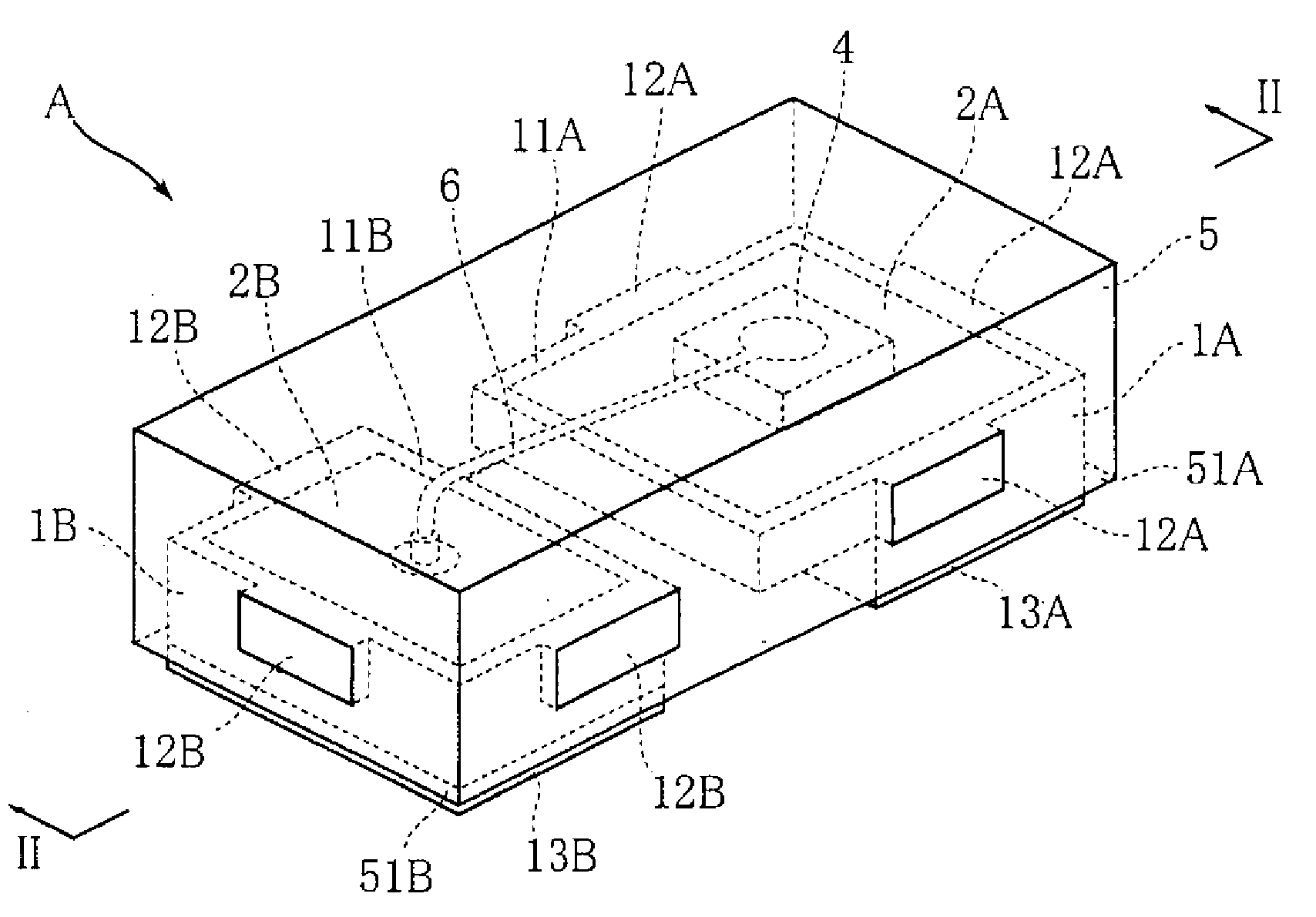
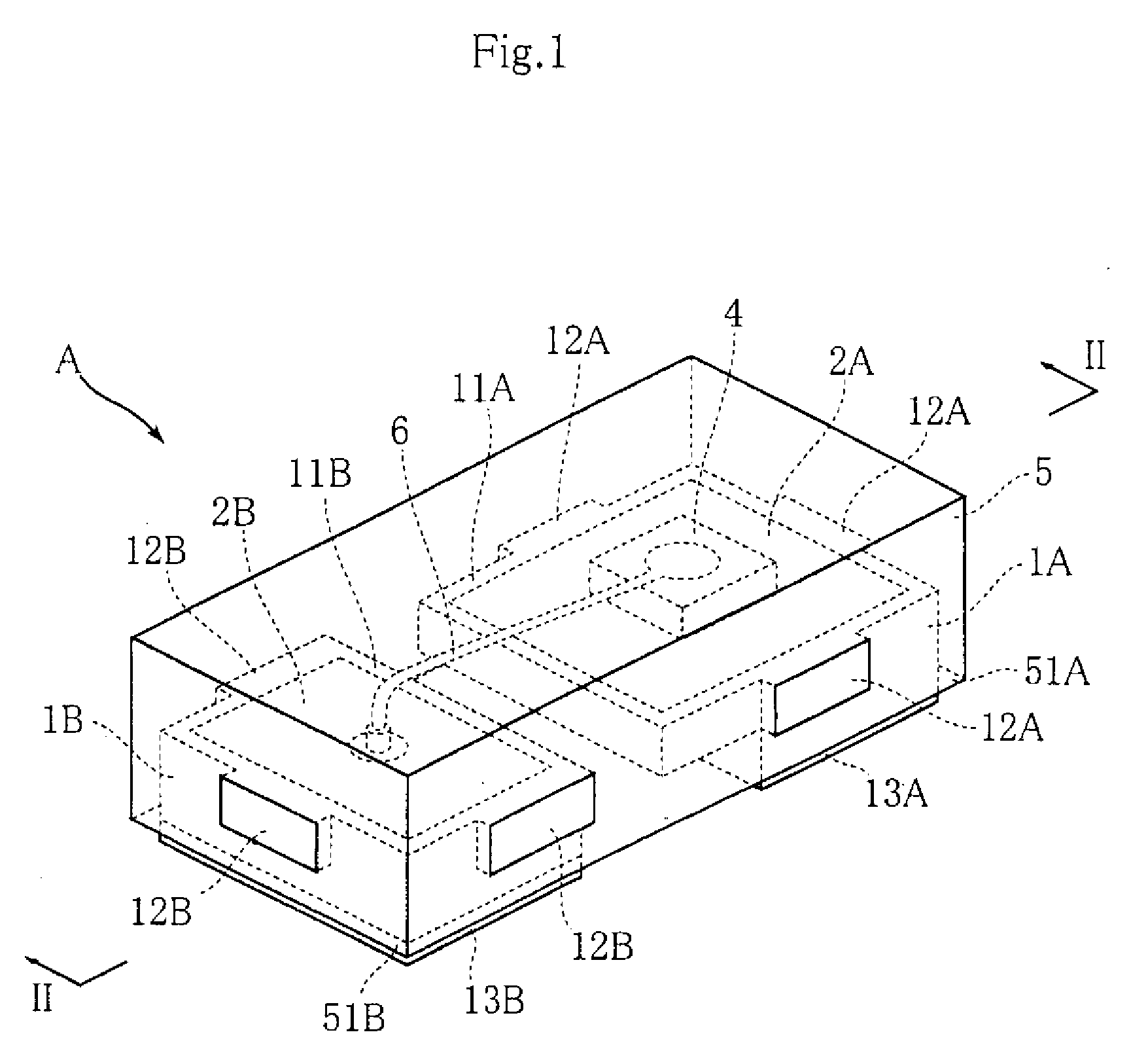
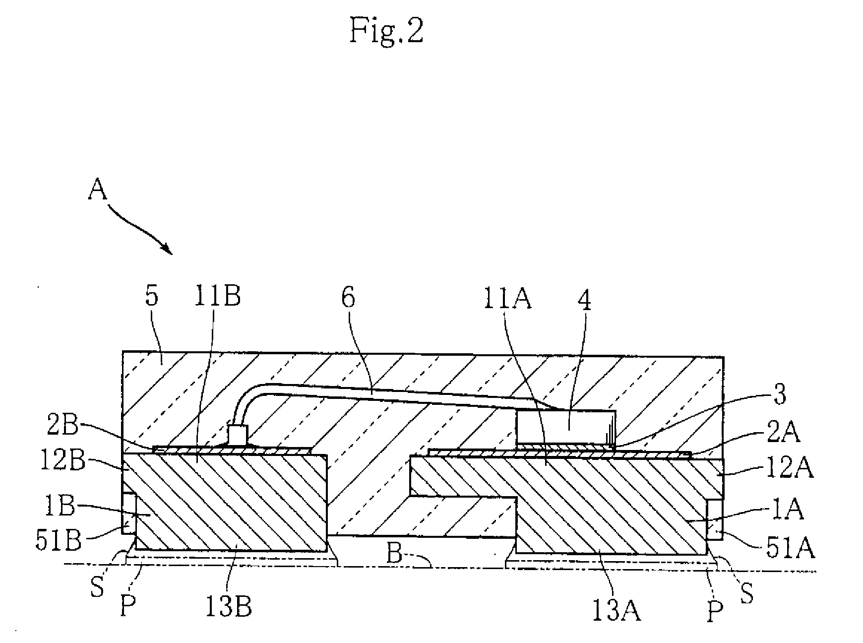
[0017]FIGS. 1-3 show a semiconductor light emitting device according to the present invention. The illustrated semiconductor light emitting device A comprises one pair of leads 1A, 1B, Ag plating layers 2A, 2B, a metal bonding layer 3, an LED chip 4, and a resin package 5. As seen from FIG. 1, in the present embodiment, the resin package 5 has a rectangular parallelepiped shape, and has an upper surface and a bottom surface which are separated in the thickness direction. Moreover, the resin package 5 has a pair of end surfaces and a pair of side surfaces which extend between the upper surface and the bottom surface. The pair of end surfaces are surfaces which are mutually separated in the lengthwise direction of the resin package 5 (the direction in which the leads 1A and 1B are mutually separated), and the pair of side surfaces are surfaces which are mutually separated in the breadthways direction of the resin package 5 (the direction which is perpendicular to both the thickness di...


PUM


Abstract

A semiconductor light emitting device (A) includes a resin package (5), a semiconductor light emitting element (4), a first lead (1A) and a second lead (1B). The resin package (5) has an upper surface and a bottom surface, and has translucency. The semiconductor light emitting element (4) is covered with the resin package (5) in a state where the semiconductor light emitting element faces the upper surface of the resin package (5). The first lead (1A) includes a bonding pad (11A) which supports the semiconductor light emitting element (4). The second lead (1B) is separated from the first lead (1A), and is electrically connected to the semiconductor light emitting element (4) via a wire (6). The leads (1A, 1B) have mounting terminals (13A, 13B) which are exposed from the bottom surface of the resin package (5). The mounting terminals (13A, 13B) are surrounded by the resin package (5) in an in-plane direction perpendicular to the thickness direction of the resin package.

Description

TECHNICAL FIELD[0001]The present invention relates to a semiconductor light emitting device which is used as a light source in a mobile telephone or a dot matrix type image display device, for example.BACKGROUND ART[0002]FIG. 4 shows one example of a conventional semiconductor light emitting device (see Patent Document 1 described below). The semiconductor light emitting device X shown in FIG. 4 comprises a substrate 91, a pair of electrodes 92A, 92B formed on this substrate, and an LED chip 94 which is bonded to the electrode 92A. The LED chip 94 and a bonding wire 96 are covered with a resin package 95. One of the electrodes 92A includes a bonding pad 92Aa, and the LED chip 94 is connected to this bonding pad 92Aa by means of Ag paste 93. The other electrode 92B has a bonding pad 92Ba for fixing a bonding wire 94.[0003]Patent Document 1: Japanese Patent Application Laid-open No. 2001-196641[0004]The semiconductor light emitting device X having the composition described above is us...

Claims


Application Information

Patent Timeline
Patent Type & Authority Applications(United States)
IPC IPC(8): H01L33/00H01L33/48H01L33/62
CPCH01L33/486H01L33/62H01L2224/48247H01L2224/48471H01L2224/73265H01L2224/32225H01L2224/32245H01L2924/01322H01L2224/48227H01L2924/00H01L2224/48091H01L2924/00014H01L2924/00012
Inventor ITAI, JUNICHI
Owner ROHM CO LTD
Why Eureka
Try Eureka