Eureka AIR delivers breakthrough ideas for toughest innovation challenges, trusted by R&D personnel around the world.

Imprinting mold and pattern formation method

Inactive Publication Date: 2010-07-01
KK TOSHIBA
View PDF2 Cites 11 Cited by
  • Summary
  • Abstract
  • Description
  • Claims
  • Application Information

AI Technical Summary

Benefits of technology

[0009]According to a first aspect of the invention, there is provided an imprint mold comprising: a substrate; a concave and convex pattern provided on the substra

Problems solved by technology

However, this technique is still in the research stage, and there are many problems to be solved to put the technique to practical use.
Unfortunately, the conventional imprint lithography has the following problems.
That is, when the mold is released, the imprinting agent breaks and remains in the concave and convex pattern of the mold, thereby causing a so-called mold defect.
If this defect once occurs, the defect repeats because the next imprinting (shot) is performed using the same mold in imprint lithography, and this worsens the yield.
In addition, it is difficult to remove the imprinting agent remaining in the concave and convex pattern of the mold if no appropriate cleaning is performed.

Method used


Image

  • Imprinting mold and pattern formation method
  • Imprinting mold and pattern formation method
  • Imprinting mold and pattern formation method

Examples


first embodiment

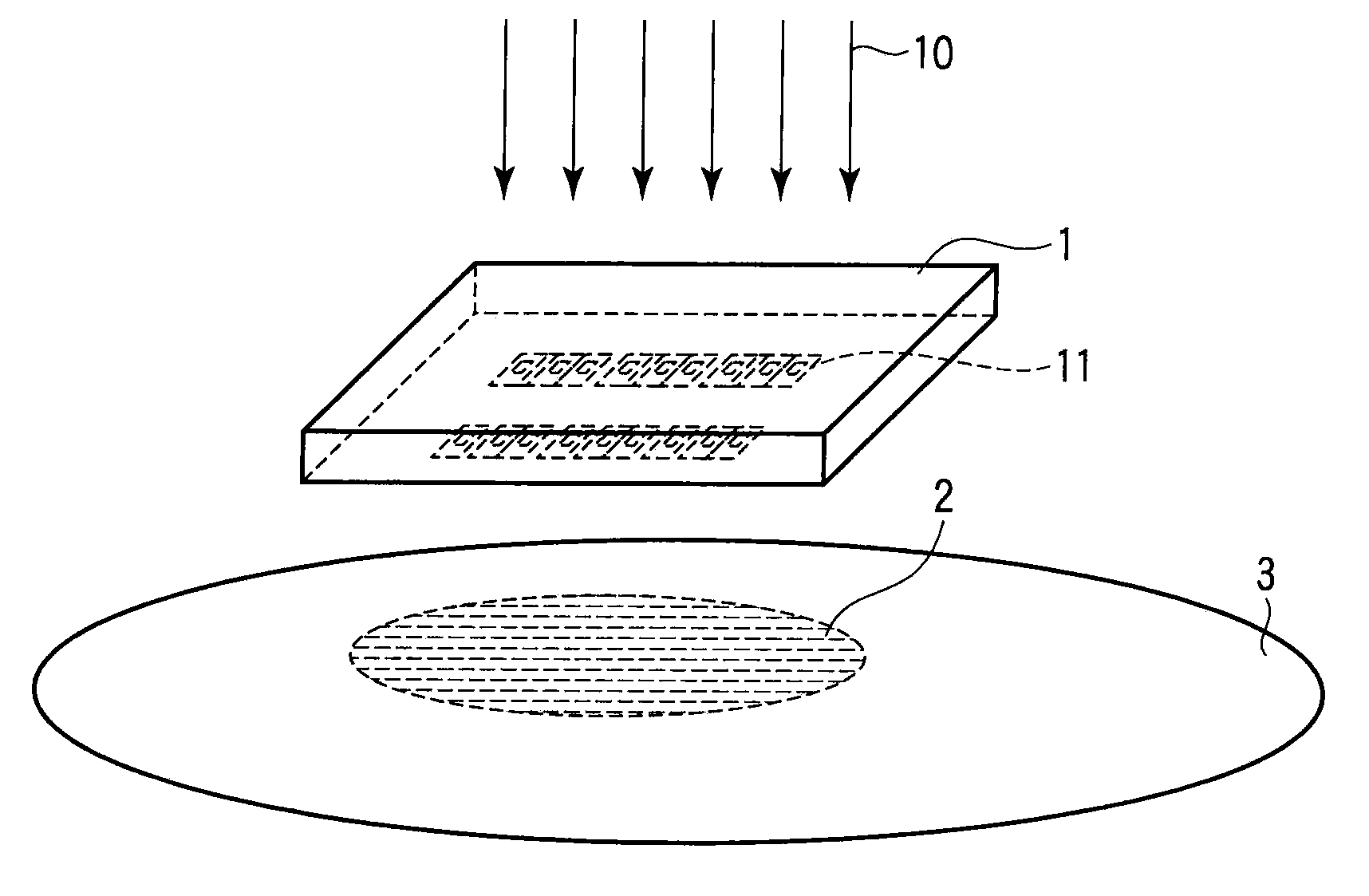
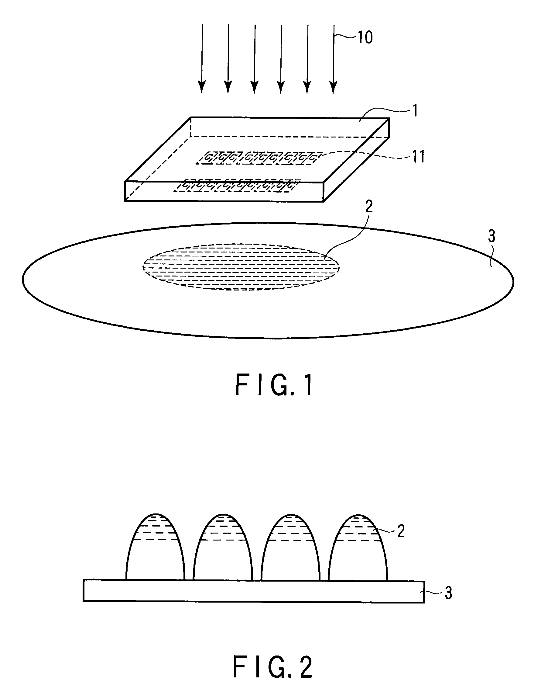
[0035]FIG. 1 is a view showing the positional relationship between a mold 1 for optical imprinting, a concave and convex pattern 11 formed on the mold 1 and corresponding to a pattern to be transferred, an imprinting agent 2 coated on a substrate 3 to be processed, and light 10 for curing the imprinting agent 2. FIGS. 2 to 6 are sectional views for explaining a pattern formation method of this embodiment. These sectional views are equivalent to side views of FIG. 1.

[FIG. 2]

[0036]The imprinting agent 2 is applied on the substrate 3 to be processed.

[0037]In this embodiment, the imprinting agent 2 is a photocuring resin (photocuring imprinting agent). Also, in this embodiment, the imprinting agent 2 is applied shot by shot by an inkjet method. Note that the method of this embodiment is also applicable to a method by which the entire surface of the substrate 3 is coated with the imprinting agent 2 by spin coating.

[0038]The substrate 3 to be processed is a semiconductor substrate such as...

second embodiment

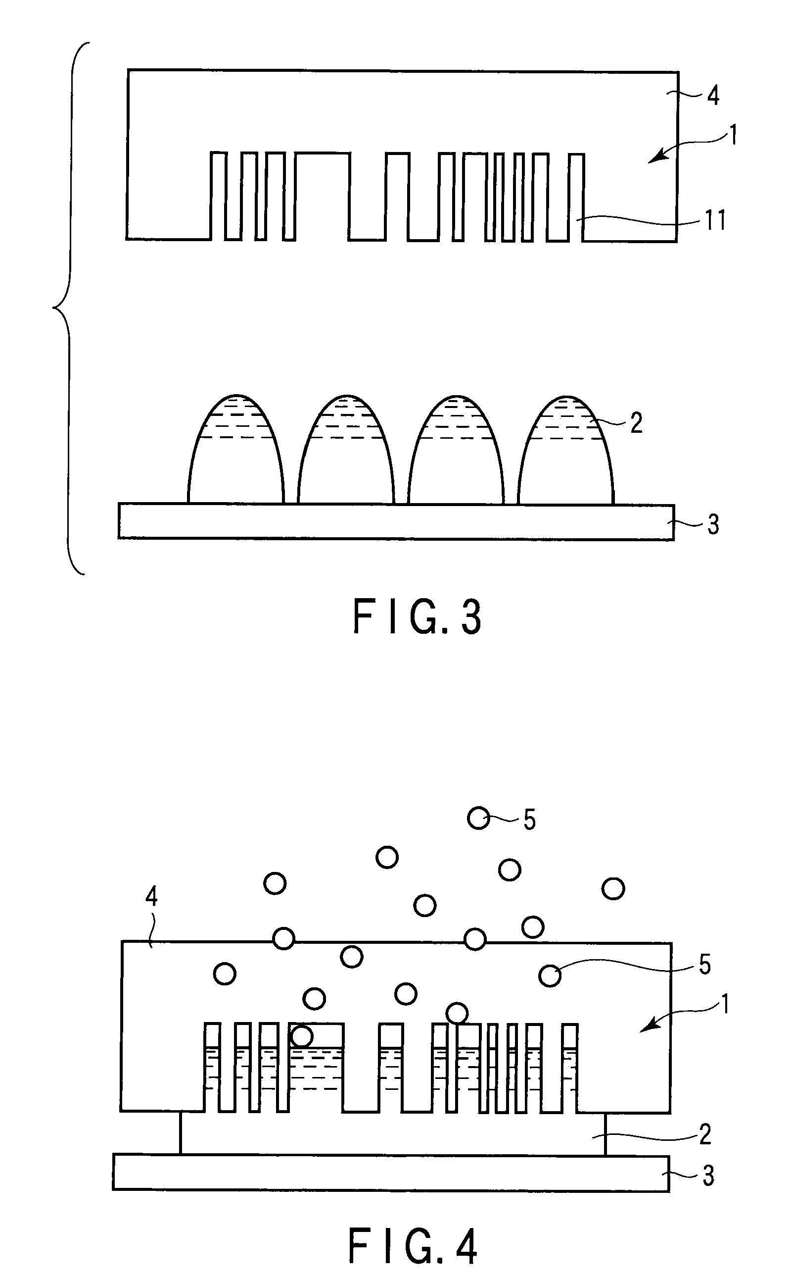
[0058]FIGS. 7 and 8 are sectional views for explaining a pattern formation method according to the second embodiment of the present invention. Note that the same reference numerals as in the above-mentioned drawing denote the same parts in the following drawing, and a repetitive explanation will be omitted.

[0059]The difference of this embodiment from the first embodiment is to positively control a gas permeating through a mold 1.

[0060]FIG. 7 shows a method by which in the step of releasing the mold 1, the ambient pressure on the upper surface of the mold 1 is made higher than that between the mold 1 and an imprinting agent 2, and the pressure between the mold 1 and imprinting agent 2 is raised by injecting a gas 5 between them so as to force the cured imprinting agent 2 out of the mold 1, thereby more effectively suppressing the occurrence of a mold defect.

[0061]FIG. 8 shows a method by which in the step of filling the imprinting agent 2 in a concave and convex pattern of the mold 1...

third embodiment

[0062]FIG. 9 is a sectional view for explaining a pattern formation method according to the third embodiment of the present invention.

[0063]The difference of this embodiment from the first embodiment is to use a mold 1 containing a gas 5 to such an extent that the gas 5 is saturated. Since the mold 1 containing the gas 5 is used, the gas 5 in the mold 1 leaks in the step of filling an imprinting agent 2, thereby forming a gas layer 51 between the mold 1 and imprinting agent 2. This makes it possible to prevent the imprinting agent 2 from partially remaining in recesses of the mold 1, and obtain the same effect as that of the first embodiment. The method of this embodiment has the advantage that even when the gas permeability of the mold 1 itself is low, the occurrence of a mold defect can effectively be suppressed by the assistance of the gas layer 51.

[0064]The same effect can also be obtained by forming the gas layer 51 between the mold 1 and imprinting agent 2 by holding the gas p...


PUM

PropertyMeasurementUnit
Pressureaaaaaaaaaa
Flow rateaaaaaaaaaa
Sizeaaaaaaaaaa

Abstract

An imprint mold includes a substrate, a concave and convex pattern provided on the substrate and corresponding to a pattern to be transferred, and a gas permeable region having higher gas permeability than molten quartz in which impurities are not doped.

Description

CROSS-REFERENCE TO RELATED APPLICATIONS[0001]This application is based upon and claims the benefit of priority from prior Japanese Patent Application No. 2008-333077, filed Dec. 26, 2008, the entire contents of which are incorporated herein by reference.BACKGROUND OF THE INVENTION[0002]1. Field of the Invention[0003]The present invention relates to an imprinting mold for use in imprint lithography, and a pattern formation method using the same.[0004]2. Description of the Related Art[0005]In the fabrication process of an advanced semiconductor product, the degree of micropatterning is increased by mainly increasing the resolution of an exposure apparatus. The resolution of an exposure apparatus is determined by the wavelength of exposure light and the numerical aperture (NA) of a projection lens; the shorter the wavelength and the higher the NA, the higher the resolution. Recently, deep ultraviolet light having a wavelength of 193 nm is used. Also, although a theoretically highest va...

Claims


Application Information

Patent Timeline
IPC IPC(8): B29C59/16B28B11/08B29C59/02
CPCB29C35/0888B29C37/0003B29C37/0053B29C37/006B29C43/003B29C43/021B29C2035/0827B29C2043/025B29C2043/3634B29C2059/023B29K2105/0002B82Y10/00B82Y40/00G03F7/0002
Inventor FURUTONO, YOHKOINANAMI, RYOICHINOMURA, HIROSHI
Owner KK TOSHIBA
Why Eureka
Eureka Blog
Learn More