Supercharge Your Innovation With Domain-Expert AI Agents!

Display device

Active Publication Date: 2010-07-15
PANASONIC LIQUID CRYSTAL DISPLAY CO LTD +1
View PDF4 Cites 13 Cited by
  • Summary
  • Abstract
  • Description
  • Claims
  • Application Information

AI Technical Summary

Benefits of technology

[0007]The invention has been made under such circumstances, and it is an object of the invention to provide a display device which can realize the reduction of EMI generated during charge sharing drive of a charge in a driver circuit which controls the supply of a charge to array of cells which can store the charge.

Problems solved by technology

Particularly, with respect to a touch-panel-type liquid crystal display device in which a touch panel screen functions as an input device when a finger of a user or the like touches the touch panel screen, the touch panel screen is arranged close to a liquid crystal display screen and hence, the touch panel screen is liable to be influenced by the EMI generated on the display screen whereby an erroneous operation is induced due to erroneous recognition of positional coordinates.

Method used


Image

  • Display device
  • Display device
  • Display device

Examples


first embodiment

[0035]Hereinafter, the invention is explained in conjunction with FIG. 1 to FIG. 9.

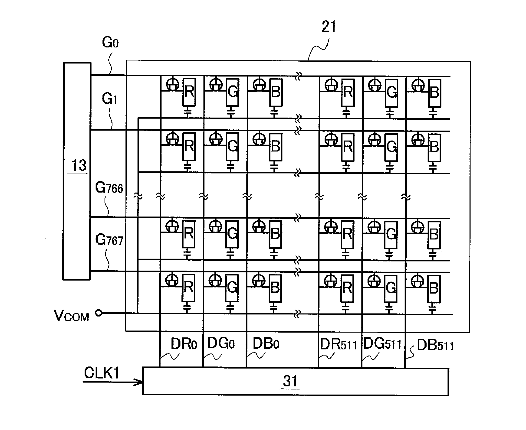
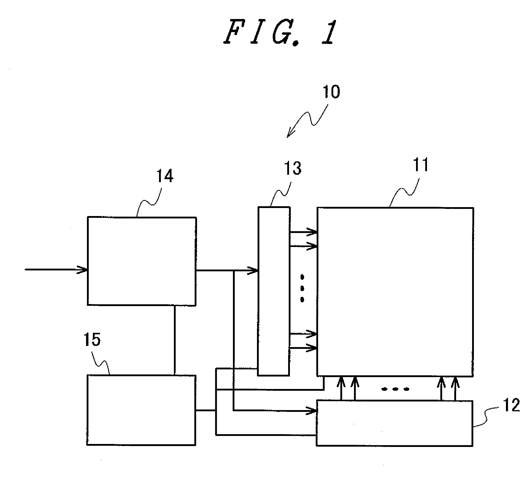
[0036]FIG. 1 schematically shows the constitution of a TFT (Thin Film Transistor) liquid crystal display device 10 including a driver circuit according to one embodiment of the invention. This liquid crystal display device 10 is constituted of (a) a liquid crystal panel 11 which includes TFTs (thin film transistors) and visually displays an image thereon by operating the TFTs, (b) a source driver part 12 which controls a voltage applied to drain terminals of the TFTs formed on the liquid crystal panel 11, (c) a gate driver part 13 which controls a voltage applied to gate terminals of the TFTs formed on the liquid crystal panel 11, (d) a display control circuit 14 which receives image data to be displayed and instructs the source driver part 12 and the gate driver part 13 to perform operations respectively, and (e) a power source circuit 15 which supplies electricity to the liquid crystal panel 11, the...

second embodiment

[0045]Hereinafter, the invention is explained in conjunction with FIG. 10.

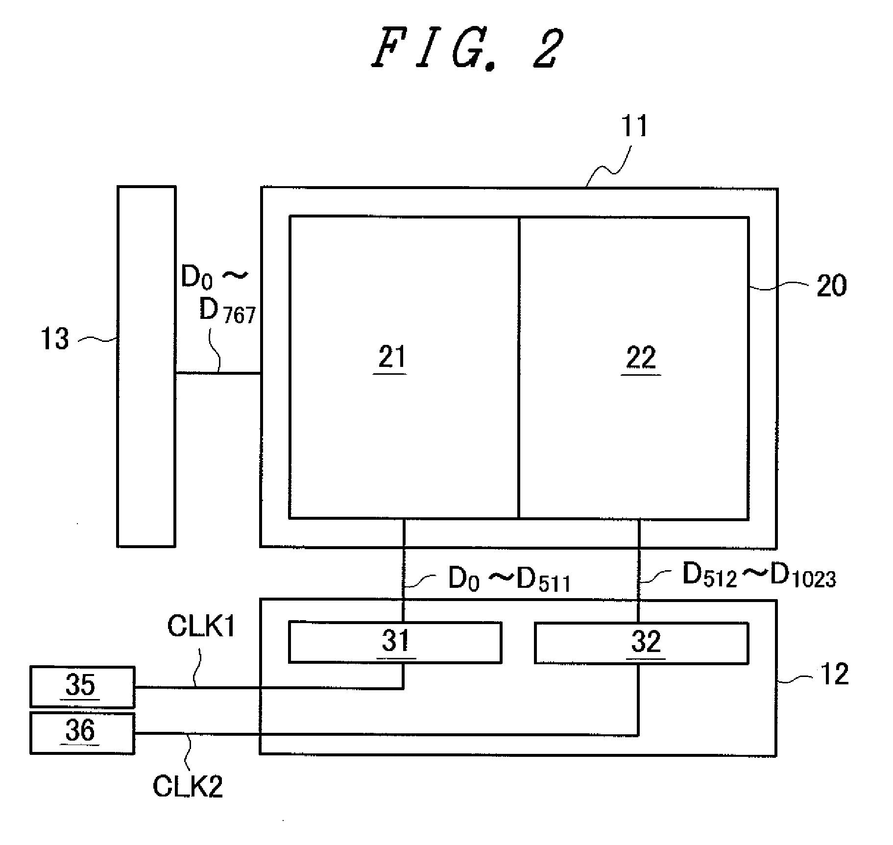
[0046]In the above-mentioned first embodiment, the TFT array substrate 20 is divided into two regions consisting of the region 21 and the region 22. However, as shown in FIG. 10, the TFT array substrate 20 may be divided into four regions consisting of regions 121 to 124. In this case, as shown in the drawing, clock signals CLK1, CLK2 are respectively divided and divided signals are respectively inputted alternately to a first drive part 131 to a fourth drive part 134 which control the drain signals D supplied to the regions 121 to 124. Accordingly, the EMI which occurs simultaneously can be dispersed thus reducing the EMI as a whole. Further, the invention is not limited to the above-mentioned embodiment, and a case where the number of division of the TFT array substrate exceeds four and a case where clock signals which differ in timing are applied to drive parts also fall within the scope of the technical co...

third embodiment

[0047]Hereinafter, the invention is explained in conjunction with FIG. 11.

[0048]FIG. 11 schematically shows a touch-panel-type liquid crystal display device 50 which uses the liquid crystal panel 1 according to the above-mentioned first embodiment or second embodiment. As shown in FIG. 11, the touch-panel-type liquid crystal display device 50 includes: (i) a liquid crystal panel 11 having the structure substantially equal to the structure of the liquid crystal panel according to the first embodiment or second embodiment; (ii) a touch panel part 51 which functions as an input device when a finger of a user or the like touches the touch panel part 51; (iii) a backlight unit 52 which radiates light from a back surface side of the liquid crystal panel 11; (iv) a metal frame portion 53 which constitutes a housing of the touch-panel-type liquid crystal display device 50; (v) a flexible printed circuit board 54 which constitutes a film-like wiring circuit such as a COF (Chip On Film) or a ...


PUM


Abstract

In a driver circuit which controls the supply of charge to cells each of which can store a charge, the EMI (Electro Magnetic Interference) which occurs at the time of performing the charge sharing driving can be reduced. A preceding conduction means (SW13) which is controlled in response to a clock signal (CLK1) makes an output signal line corresponding to a first circuit which has positive polarity of a potential higher than a reference potential and an output signal line corresponding to a second circuit which has negative polarity of a potential lower than the reference potential electrically conductive with each other. After a lapse of a predetermined time, a succeeding conduction means (SW23) which is controlled in response to a clock signal (CLK2) makes an output signal line corresponding to a third circuit which has the positive polarity and an output signal line corresponding to a fourth circuit which has the negative polarity electrically conductive with each other.

Description

CROSS-REFERENCE TO RELATED APPLICATIONS[0001]The present application claims priority from Japanese application JP 2009-005368 filed on Jan. 14, 2009, the content of which is hereby incorporated by reference into this application.BACKGROUND OF THE INVENTION[0002]1. Field of the Invention[0003]The present invention relates to a display device, and more particularly to a driver circuit which controls the supply of a charge to cells of a liquid crystal display panel, an organic EL or the like which can store the charge, a display device which uses the driver circuit, and an output signal control method.[0004]2. Background Art[0005]As an information communication terminal of a computer or the like or a display device of a television receiver set, a liquid crystal display device has been popularly used. The liquid crystal display device is a device which controls an image to be displayed by changing transmissivity of light by changing the alignment of liquid crystal molecules hermetically...

Claims


Application Information

Patent Timeline
IPC IPC(8): G09G5/00G09G3/36
CPCG09G2330/023G09G3/36
Inventor YAMAGISHI, YASUHIKOMISONOU, TOSHIKI
Owner PANASONIC LIQUID CRYSTAL DISPLAY CO LTD
Features
  • R&D
  • Intellectual Property
  • Life Sciences
  • Materials
  • Tech Scout
  • Unparalleled Data Quality
  • Higher Quality Content
  • 60% Fewer Hallucinations
Learn More