Stacked Integrated Chips and Methods of Fabrication Thereof

Active Publication Date: 2010-07-15
TAIWAN SEMICON MFG CO LTD
View PDF24 Cites 105 Cited by
  • Summary
  • Abstract
  • Description
  • Claims
  • Application Information

AI Technical Summary

Benefits of technology

[0008]These and other problems are generally solved or circumvented, and technical a

Problems solved by technology

However, three-dimensional integration introduces many challenges to fabrication.
One of the challenges in three-dimensional integration involves forming joints between the stacked substrates without forming additional shorts or

Method used


Image

  • Stacked Integrated Chips and Methods of Fabrication Thereof
  • Stacked Integrated Chips and Methods of Fabrication Thereof
  • Stacked Integrated Chips and Methods of Fabrication Thereof

Examples


Embodiment Construction

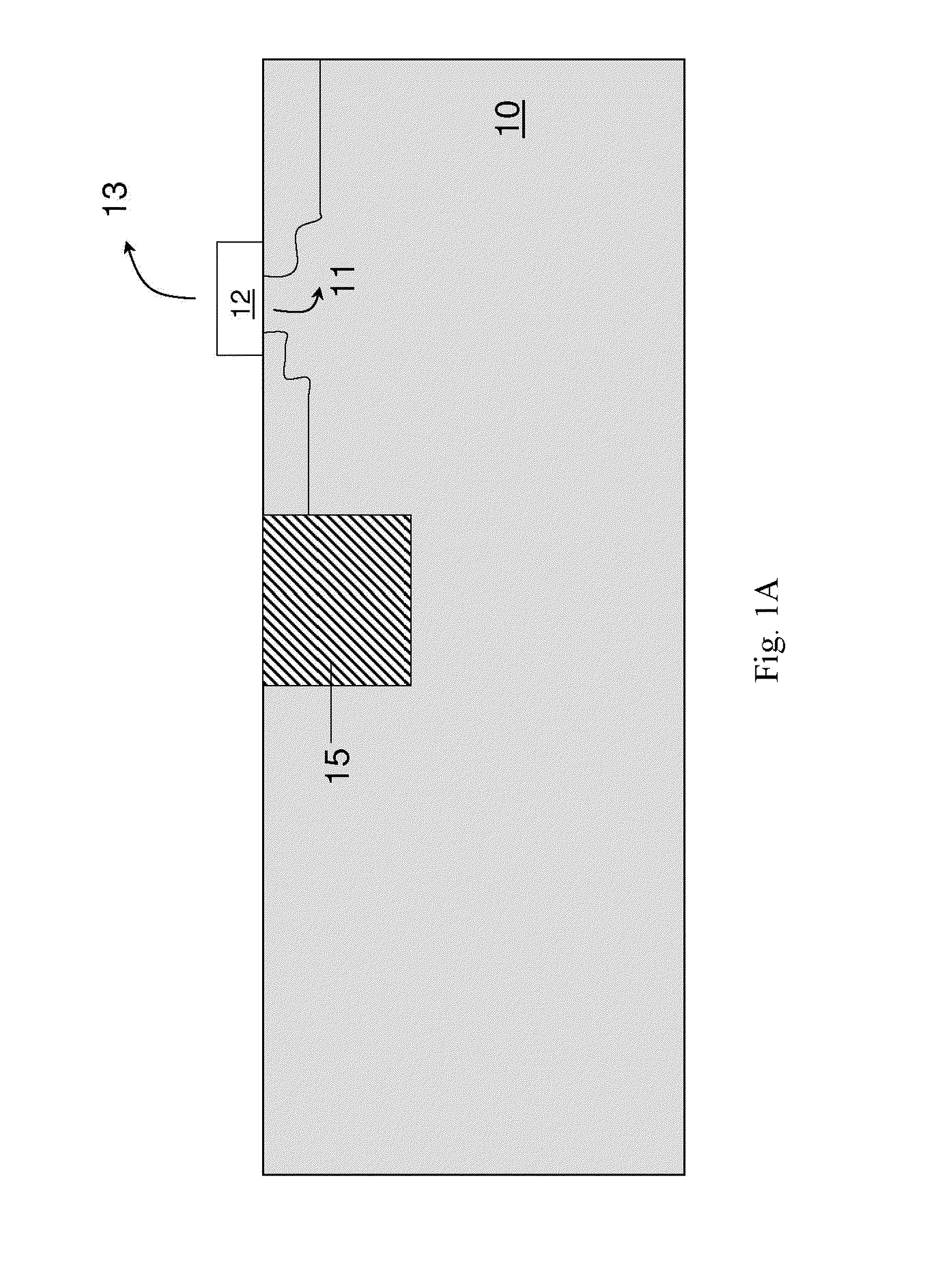
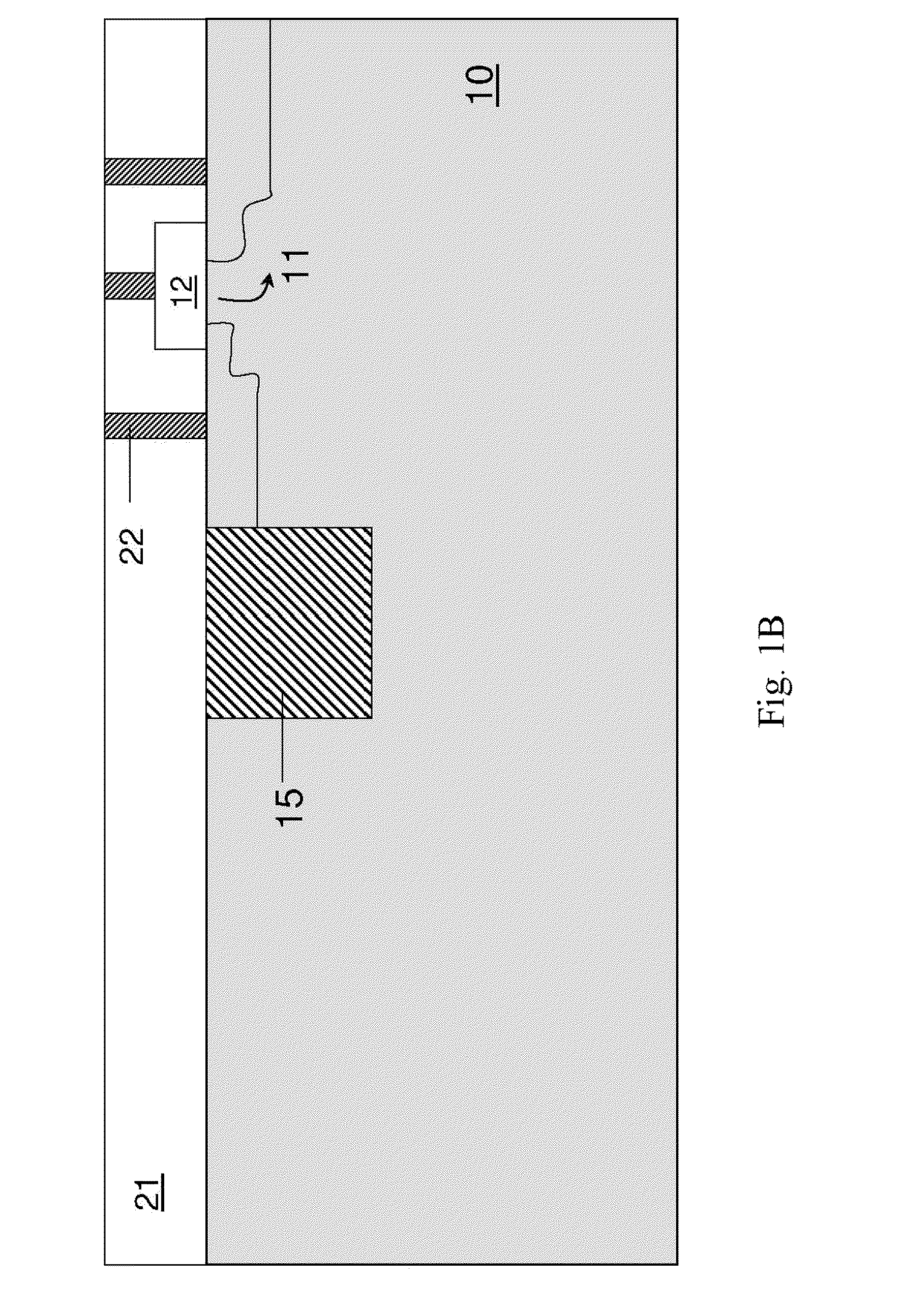
[0016]The making and using of the presently preferred embodiments are discussed in detail below. It should be appreciated, however, that the present invention provides many applicable inventive concepts that can be embodied in a wide variety of specific contexts. The specific embodiments discussed are merely illustrative of specific ways to make and use the invention, and do not limit the scope of the invention.

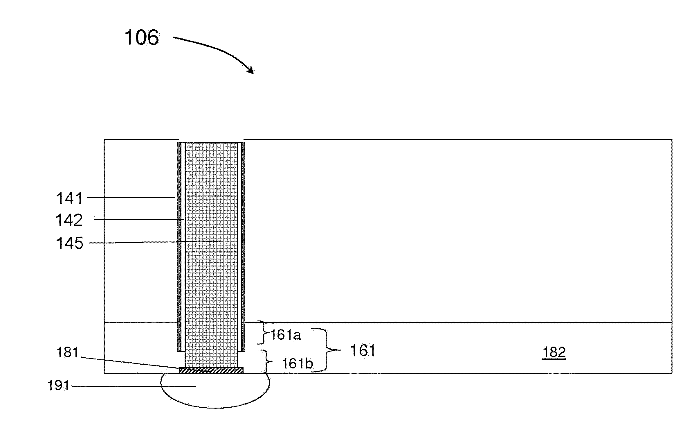
[0017]The through substrate vias are insulated from the substrate by a dielectric layer. A through substrate via from one chip is joined to a suitable landing pad or an under bump structure of another substrate using, for example, solder balls. However, some of the conductive materials used in the joining process may form a conductive string between the joint and the substrate thus electrically coupling the through substrate via to the substrate. In various embodiments, the invention avoids this electrical shorting by the use of a sidewall spacer that only exposes a portion o...


PUM


Abstract

Structure and methods of forming stacked semiconductor chips are described. In one embodiment, a method of forming a semiconductor chip includes forming an opening for a through substrate via from a top surface of a first substrate. The sidewalls of the opening are lined with an insulating liner and the opened filled with a conductive fill material. The first substrate is etched from an opposite bottom surface to form a protrusion, the protrusion being covered with the insulating liner. A resist layer is deposited around the protrusion to expose a portion of the insulating liner. The exposed insulating liner is etched to form a sidewall spacer along the protrusion.

Description

[0001]This application claims the benefit of U.S. Provisional Application No. 61 / 144,389 filed on Jan. 13, 2009, entitled “Stacked Integrated Chips and Methods of Fabrication Thereof,” which application is hereby incorporated herein by reference.TECHNICAL FIELD[0002]The present invention relates generally to integrated chips, and more particularly to stacked integrated chips and methods of fabrication of stacked integrated chips.BACKGROUND[0003]Semiconductor devices are manufactured by forming active regions in a semiconductor substrate, depositing various insulating, conductive, and semiconductive layers over the substrate, and patterning them in sequential steps. The upper or last-formed layers of the semiconductor device typically comprise metallization layers. The metallization layers typically comprise one or more layers of metal interconnect having conductive lines disposed within an insulating material and may provide connections to underlying active regions and connections w...

Claims


Application Information

Patent Timeline
IPC IPC(8): H01L21/768
CPCH01L21/76898H01L23/49816H01L25/50H01L2225/06513H01L2225/06517H01L2225/06541H01L2924/15311H01L2224/16145H01L2224/16225H01L2224/32225H01L2224/73204H01L25/0657H01L2924/1305H01L2924/18161H01L23/49827H01L2924/00012H01L2924/00H01L2224/05009H01L2224/05025H01L2224/0557H01L2224/05001H01L2224/05124H01L2224/05139H01L2224/05144H01L2224/05147H01L2224/05166H01L2224/05181H01L2224/05184H01L2224/05644H01L2224/05655H01L2224/05571H01L2224/16146H01L24/05H01L24/03H01L2224/02372H01L2224/13025H01L2924/00014
Inventor CHEN, MING-FAHUANG, JAO SHENG
Owner TAIWAN SEMICON MFG CO LTD
Why Eureka
Try Eureka