Semiconductor device and method of manufacturing the same

a technology of semiconductor devices and semiconductors, applied in the direction of semiconductor devices, basic electric elements, electrical equipment, etc., can solve the problems of degrading the yield of vertical mos transistors, fluctuation of gate lengths, etc., and achieve the effect of preventing fluctuation of transistor characteristics and preventing gate length fluctuations

Inactive Publication Date: 2010-07-22
ELPIDA MEMORY INC
View PDF1 Cites 21 Cited by
  • Summary
  • Abstract
  • Description
  • Claims
  • Application Information

AI Technical Summary

Benefits of technology

[0014]Accordingly, a fluctuation in the gate length can be prevented, thereby pre...

Problems solved by technology

However, uneven etching causes a fluctuation in the gate length of the vertical MOS transistor.
Consequently...

Method used


Image

  • Semiconductor device and method of manufacturing the same
  • Semiconductor device and method of manufacturing the same
  • Semiconductor device and method of manufacturing the same

Examples


Embodiment Construction

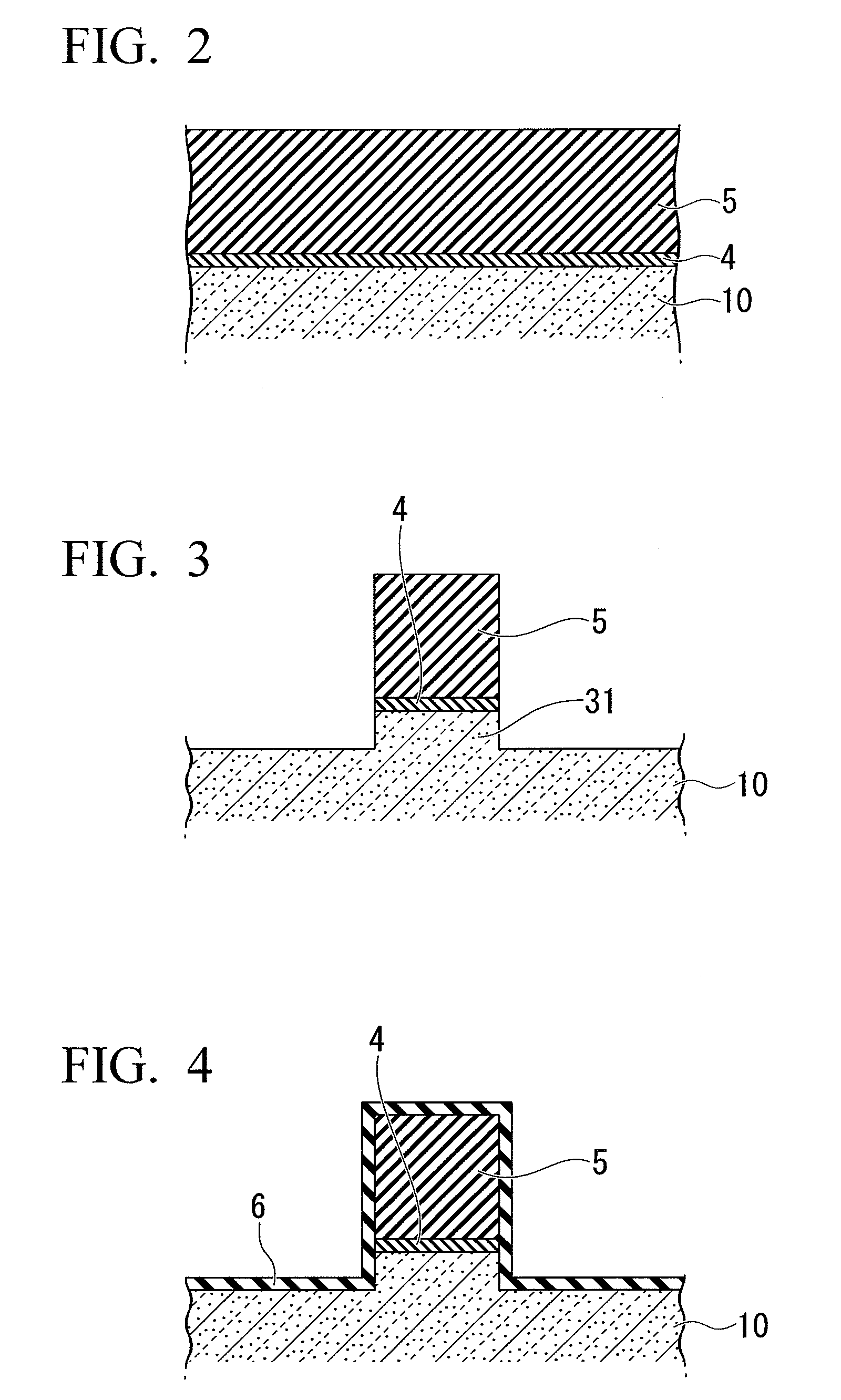
[0023]The present invention will now be described herein with reference to illustrative embodiments. The accompanying drawings explain a semiconductor device and a method of manufacturing the semiconductor device in the embodiments. The size, the thickness, and the like of each illustrated portion might be different from those of each portion of an actual semiconductor device.

[0024]Those skilled in the art will recognize that many alternative embodiments can be accomplished using the teachings of the present invention and that the present invention is not limited to the embodiments illustrated herein for explanatory purposes.

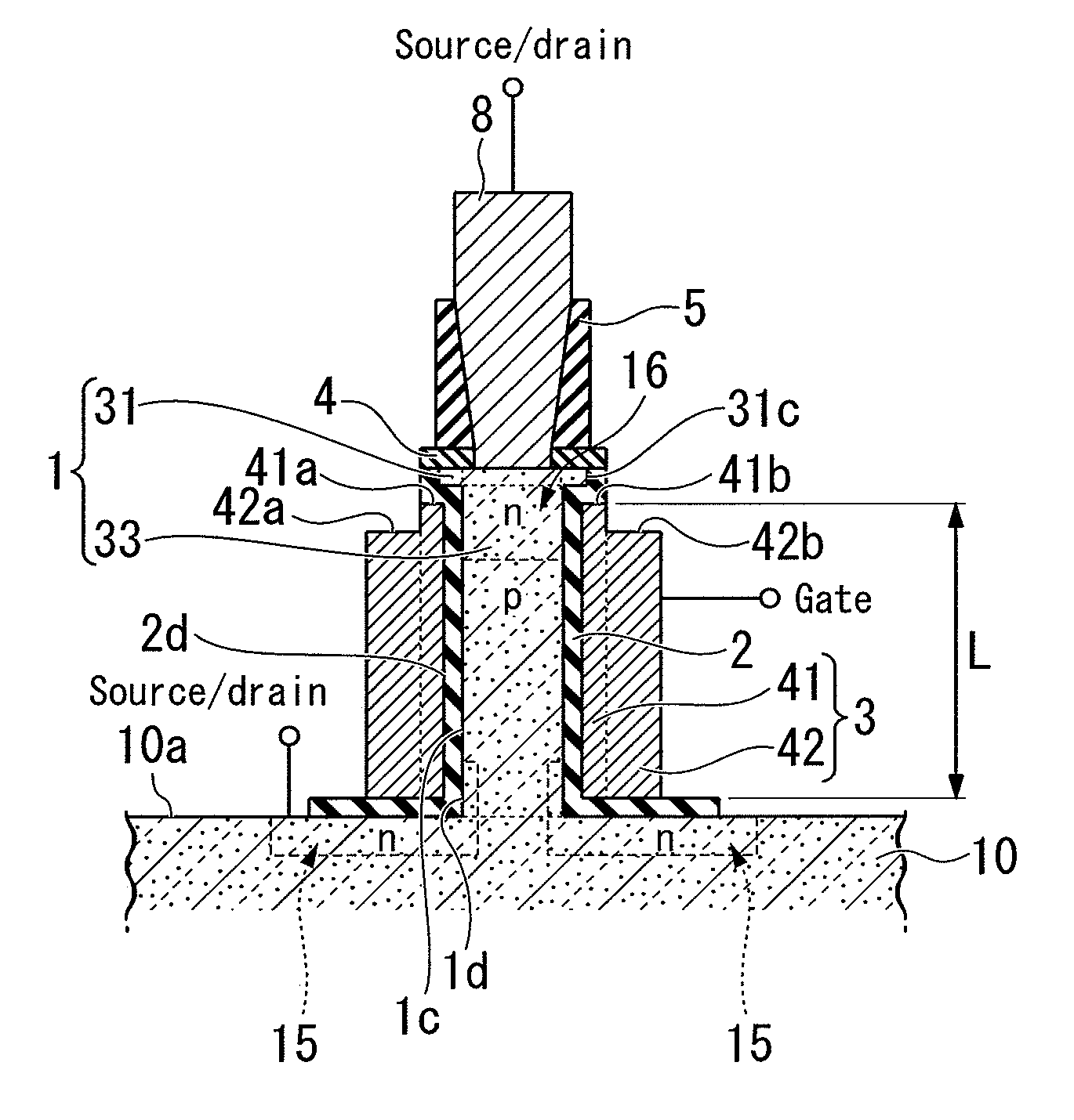
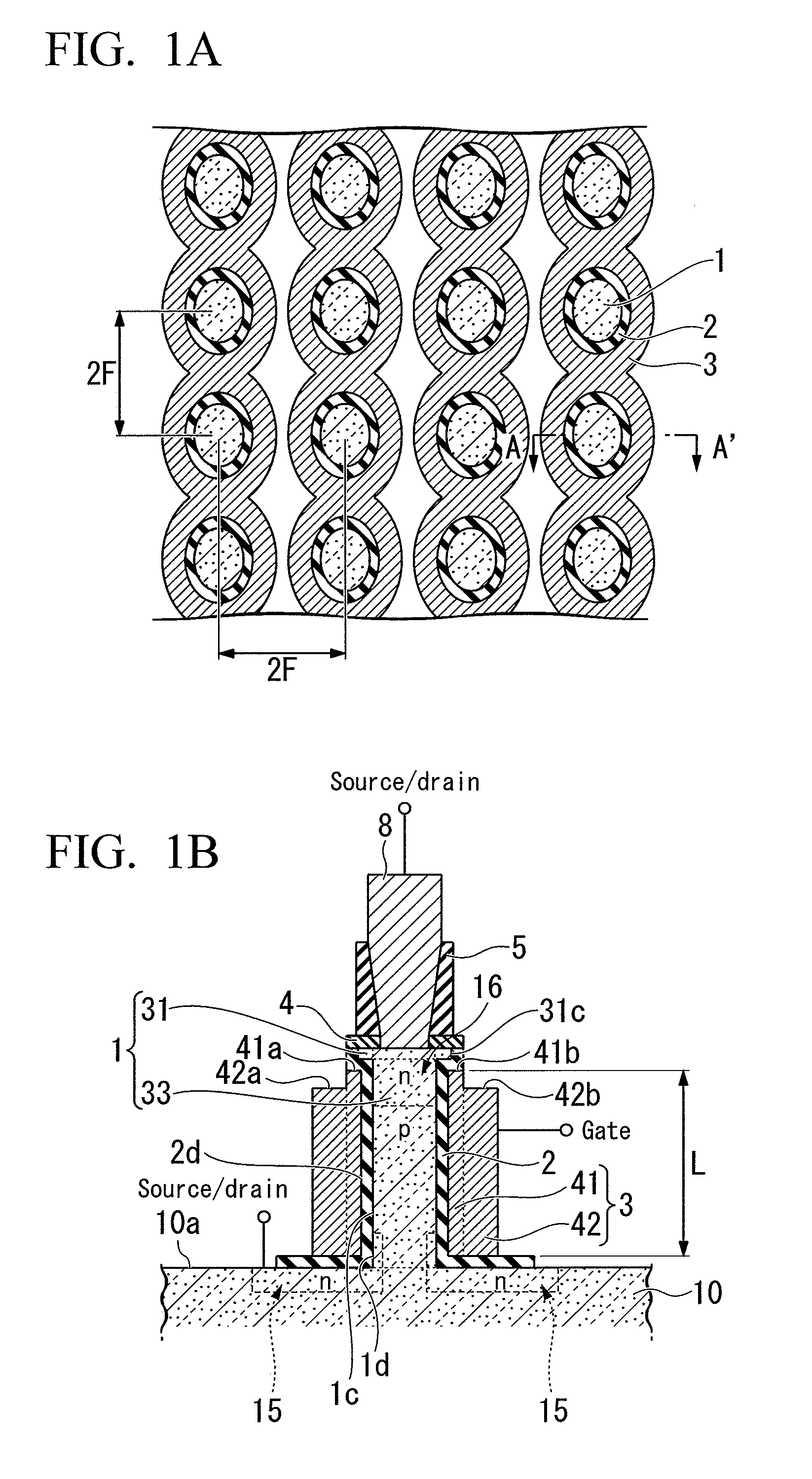
[0025]FIG. 1A is a plane view illustrating 4F2 memory cells of a semiconductor device according to a first embodiment of the present invention. FIG. 1B is a cross-sectional view taken along a line A-A′ shown in FIG. 1A.

[0026]As shown in FIG. 1A, the semiconductor device according to the first embodiment includes 4F2 memory cells including: pillars 1; first insul...


PUM


Abstract

A semiconductor device includes a semiconductor pillar, an insulator, and an electrode. The semiconductor pillar has a semiconductor portion outwardly extending. The insulator extends along the semiconductor pillar. The insulator has an insulating portion outwardly extending along the semiconductor portion. The electrode extends along the insulator. The insulator is between the semiconductor pillar and the electrode. The electrode has an electrode portion overlapping the insulating portion in plain view. The electrode portion is under the insulating portion.

Description

BACKGROUND OF THE INVENTION[0001]1. Field of the Invention[0002]The present invention relates to a semiconductor device and a method of manufacturing the same.[0003]Priority is claimed on Japanese Patent Application No. 2009-010372, filed Jan. 20, 2009, the content of which is incorporated herein by reference.[0004]2. Description of the Related Art[0005]Recently, semiconductor chips have been smaller and smaller in size to reduce costs. For example, a DRAM (Dynamic Random Access Memory) realizing the 4F2 memory cell size (F denotes a design rule) by using a vertical MOS transistor (3D pillar-type MOS transistor) has been proposed.[0006]Gate electrodes of such a vertical MOS transistor with a 4F2 memory cell size are formed by etching back. However, uneven etching causes a fluctuation in the gate length of the vertical MOS transistor. Consequently, the transistor characteristics of each vertical MOS transistor greatly fluctuate, thereby degrading their yield.[0007]As an example of a ...

Claims


Application Information

Patent Timeline
IPC IPC(8): H01L29/78H01L21/28
CPCH01L29/7827H01L29/66666
Inventor NOJIMA, KAZUHIRO
Owner ELPIDA MEMORY INC
Why Eureka
Try Eureka