Analog-to-digital converter

a converter and analog technology, applied in the direction of digital-analogue converters, instruments, cleaning using liquids, etc., can solve the problems of increasing the cost of the converter, requiring further speed-up, and reducing the cost performance, so as to achieve the effect of small area and low power

Inactive Publication Date: 2007-06-19
CYPRESS SEMICON CORP
View PDF11 Cites 34 Cited by
  • Summary
  • Abstract
  • Description
  • Claims
  • Application Information

AI Technical Summary

Benefits of technology

[0050]As typified by an LSI referred to as a system LSI or a Mixed-Signal LSI, with advancement of the hyperfine structure, there has hitherto been increased a demand for integrating, on the same chip, a CMOS digital circuit and a CMOS analog circuit. It is requested to integrate the CMOS analog circuit ensuring performance that meets a high speed property of the hyperfine CMOS digital circuit at a low cost and with low power consumption to the greatest possible degree.
[0051]For this reason, as described above, the prior art actualized the charge redistribution (or SAR) type AD converter that attains the small area size, the moderate conversion time and the moderate conversion accuracy, however, the much lower cost performance, the lower power consumption and the further speed-up are demanded of the differential charge redistribution (or SAR) type AD converter.
[0057]At the point of time when the first digital-to-analog converter and the second digital-to-analog converter take in the sample data of the first analog signal and the second analog signal, the first common terminal and the second common terminal are connected to each other by the first switch, and hence the first digital-to-analog converter and the second digital-to-analog converter can take in the sample data in a way that sets the first common terminal and the second common terminal as a common reference point. Then, when the first input switch and the second input switch are opened after the completion of taking in the sample data, the fluctuation in the electric potential of the first analog terminal and the electric potential of the second analog terminal is restrained, whereby the conversion into the digital data can be done by restraining the electric potential fluctuation as a concomitant of the take-in of the sample data even when the sample data have an amplitude that is as large as approximately a limit of the power source voltage range.
[0058]According to the invention, it is possible to provide the analog-to-digital converter capable of operating with the small area and the low power, and converting the analog input signal that is very close to the limit of the power source voltage range.

Problems solved by technology

For this reason, as described above, the prior art actualized the charge redistribution (or SAR) type AD converter that attains the small area size, the moderate conversion time and the moderate conversion accuracy, however, the much lower cost performance, the lower power consumption and the further speed-up are demanded of the differential charge redistribution (or SAR) type AD converter.
Therefore, a problem arises, wherein the power consumption in the buffer amplifier BUF1 is required with the result that the lower power consumption gets hard to attain.

Method used


Image

  • Analog-to-digital converter
  • Analog-to-digital converter
  • Analog-to-digital converter

Examples


first embodiment

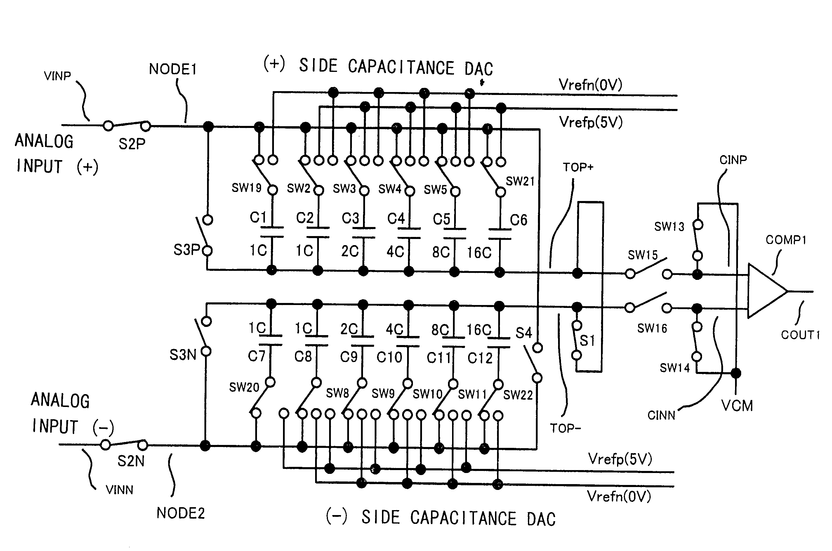
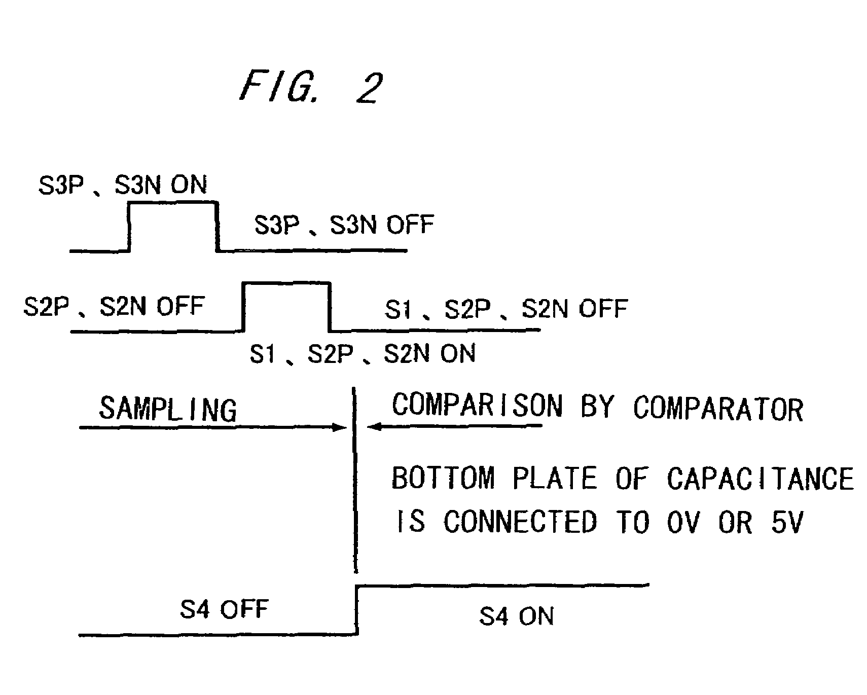
[0115]A first embodiment of the invention will hereinafter be explained in detail. FIG. 1 is a circuit diagram showing an AD converter according to the first embodiment of the invention. FIG. 2 is a diagram showing a control timing of the switches S1, S2P, S2N, S3P, S3N and S4 in FIG. 1.

[0116]In FIG. 1, SW2 through SW5, SW8 through SW11, SW13 through SW16, SW19 through SW22, S1, S2P, S2N, S3P, S3N and S4 represent switches, C1 through C12 designate capacitances, VINP indicates a (+) analog input, VINN denotes a (−) analog input, TOP+ designates a (+) side top plate of a capacitance array, TOP− represents a (−) side top plate of the capacitance array, Vrefp is a (+) side reference electric potential (e.g., 5V), Vrefn is a (−) side reference electric potential (e.g., 0V), COMP1 stands for a comparator, CINP and CINN are comparator inputs, COUT1 is an output of the comparator, VCM is a bias potential (e.g., 2.5V) of the comparator input when sampling, NODE1 and NODE2 represent internal...

second embodiment

[0164]The AD converter according to a second embodiment of the invention will be described with reference to FIG. 4. In the first embodiment, after switching OFF the switch S2P for connecting the (+) side analog input to NODE1 and the switch S2N for connecting the (−) side analog input VINN to NODE2, the fluctuations of the electric potentials of NODE1 and NODE2 are restrained by switching ON the switch S4 that equalizes the electric potentials of NODE1 and NODE2.

[0165]The second embodiment will exemplify an electric potential fluctuation restraining means that restrains the fluctuation of the electric potentials of NODE1 and NODE2 in addition to the operation of this switch S4. Alternatively, the electric potential fluctuation restraining means in the second embodiment will be exemplified as a substitute for the operation of the switch S4. In the second embodiment also, when finishing the sampling, the switches S2P, S2N for supplying the analog input signals VINP, VINN to the botto...

third embodiment

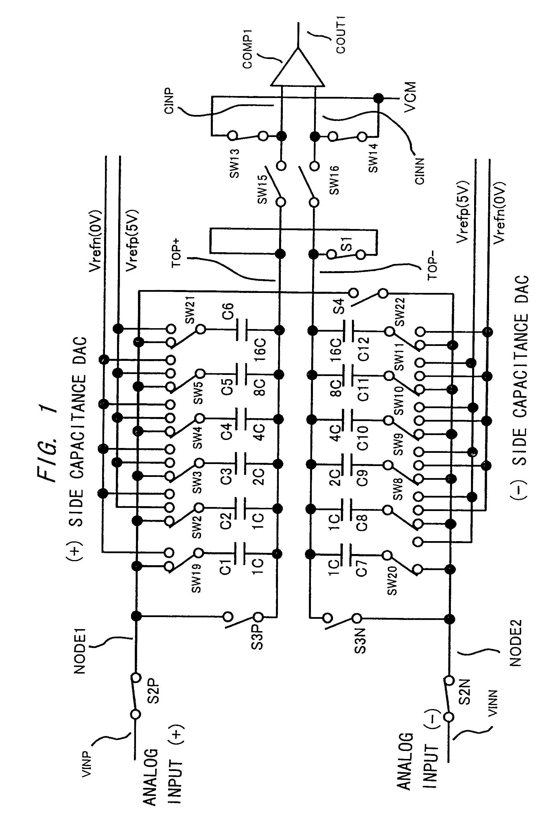
[0187]FIGS. 5 and 6 are circuit diagrams each showing an AD converter according to a third embodiment of the invention. In FIG. 5, SW2 through SW5, SW8 through SW11, SW13 through SW16, SW19 through SW22, S1, S2P, S2N, S3P, S3N and S4 represent switches, C1 through C12 designate capacitances, VINP indicates a (+) analog input, VINN denotes a (−) analog input, TOP+ designates a (+) side top plate of a capacitance array, TOP− represents a (−) side top plate of the capacitance array, Vrefp is a (+) side reference electric potential (e.g., 5V), Vrefn is a (−) side reference electric potential (e.g., 0V), COMP1 stands for a comparator, CINP and CINN are comparator inputs, COUT1 is an output of the comparator, VCM is a bias potential of the comparator input when sampling, NODE1 and NODE2 represent internal nodes, a (+) side capacitance DAC represents DAC constructed of a capacitance array of C1 through C6, and a (−) side capacitance DAC designates DAC constructed of a capacitance array of ...


PUM


Abstract

Included are a first unit including a DAC which generates a comparison signal serving as an object of comparison with the first analog signal, taking in and retaining the first analog signal, a second unit including a DAC which generates a comparison signal serving as an object of comparison with the first analog signal, taking in and retaining the second analog signal, a first switch connecting the first unit to an output side of the second unit, a comparator comparing a differential value between the first analog signal and the second analog signal with a differential value between the comparison signal of the first DAC and an output signal of the second DAC, and an electric potential control circuit controlling fluctuations in electric potentials of the first analog terminal and the second analog terminal.

Description

BACKGROUND OF THE INVENTION[0001]The invention relates to generally to an AD (analog-to-digital) converter that converts an analog signal into a digital signal, and more particularly to a differential charge redistribution (or successive approximation register (SAR)) type AD converter.[0002]Known at the present is a charge redistribution (or SAR) type AD converter having broad product applications, which is actualized with a comparatively simple circuit configuration, exhibits high compatibility with a CMOS process that can be manufactured at a comparatively low cost, and is capable of actualizing moderate conversion time and moderate conversion accuracy. Circuits disclosed in, e.g., Patent documents 1–5 and Non-Patent documents 1 and 2 are known as a conventional circuit of the charge redistribution (or SAR) type AD converter.EXAMPLE 1 OF ELECTRIC CHARGE REDISTRIBUTION TYPE AD CONVERTER[0003]FIG. 19 shows a typical differential capacitance DAC (digital-to-analog converter) of the e...

Claims


Application Information

Patent Timeline
Patent Type & Authority Patents(United States)
IPC IPC(8): H03M1/12
CPCH03M1/1023H03M1/0682H03M1/468H03M1/804
Inventor TACHIBANA, SUGURUMITSUDA, KAZUHIROKATO, TATSUO
Owner CYPRESS SEMICON CORP
Why Eureka
Try Eureka