Touch screen panel

a touch screen and panel technology, applied in the field of touch screen panels, can solve the problems of increasing complex process, and high resistance of lines, and achieve the effects of simplifying the process, reducing the resistance of intersection parts, and reducing the number of masks

Active Publication Date: 2010-07-22
SAMSUNG DISPLAY CO LTD
View PDF10 Cites 29 Cited by
  • Summary
  • Abstract
  • Description
  • Claims
  • Application Information

AI Technical Summary

Benefits of technology

[0015]It is an object of the present invention to provide a touch screen panel that removes a mask process for forming a separate coupling pattern by forming a first sensing pattern and a second sensing pattern in different layers, and by additionally forming an auxiliary metal patterns having the same material as metal patterns formed on an edge of the panel on an intersection part of the first and second sensing patterns, thereby preventing sensing sensitivity from being lowered by reducing the resistance of the intersection part.
[0019]With the present invention as describe above, the first sensing patterns coupled to each other along the first direction and the second sensing patterns coupled to each other along the second direction are disposed in different layers, making it possible to reduce the number of masks and to simplify the process. Also, substance made of the same material as the metal patterns formed on the edge of the panel is additionally formed on the intersection part of the first and second sensing patterns to reduce the resistance of the intersection part, making it possible to prevent sensing sensitivity from being lowered.

Problems solved by technology

Here, since the coupling patterns are made of the same material as the first and second sensing patterns, a mask process should be added in order to form the coupling patterns, thereby causing problems that the number of masks is increased and the process is complicated.
When the coupling pattern has a narrow width, conversely, line resistance becomes high to have a disadvantage that sensing sensitivity is lowered.

Method used


Image

  • Touch screen panel
  • Touch screen panel
  • Touch screen panel

Examples


Embodiment Construction

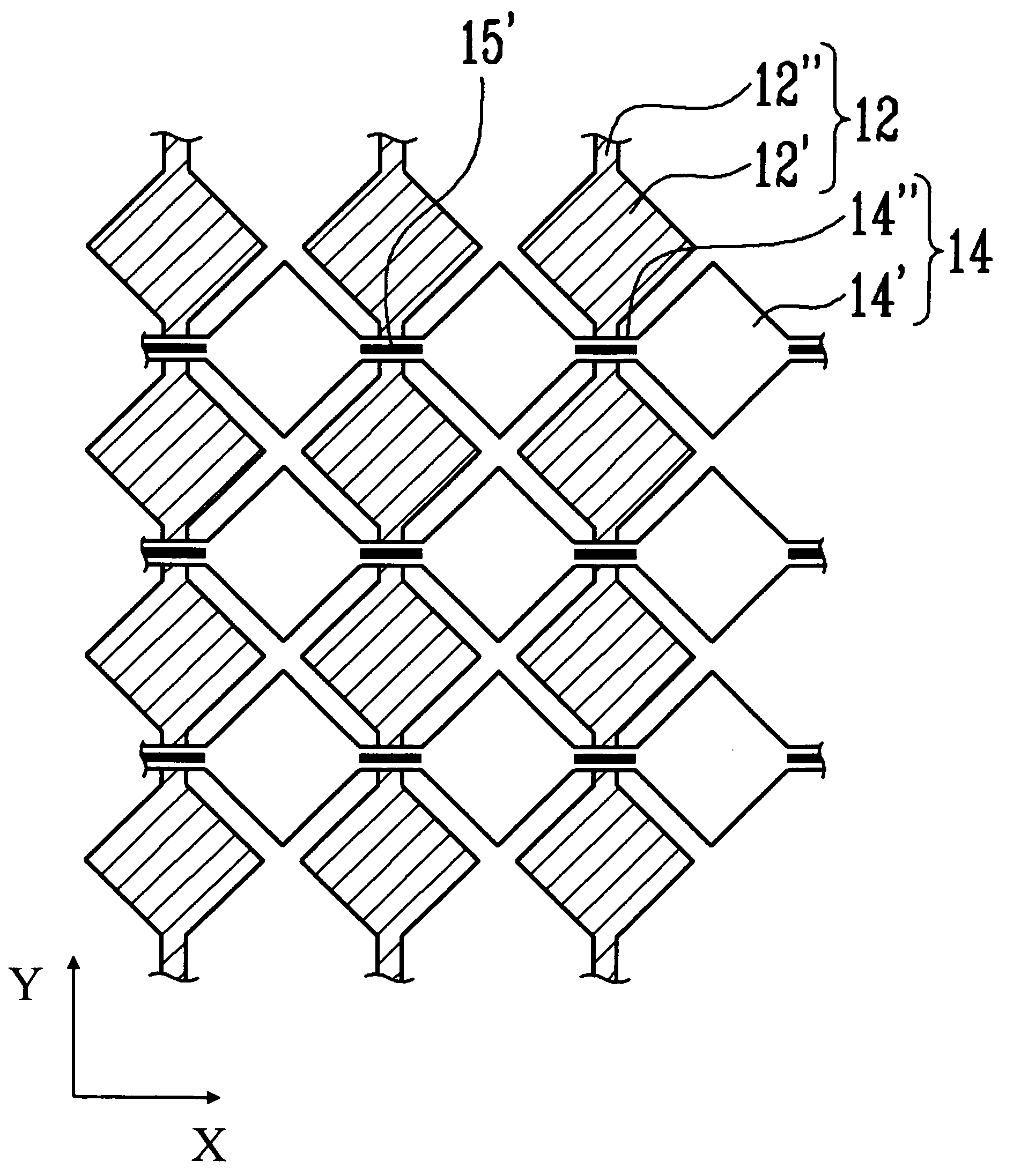
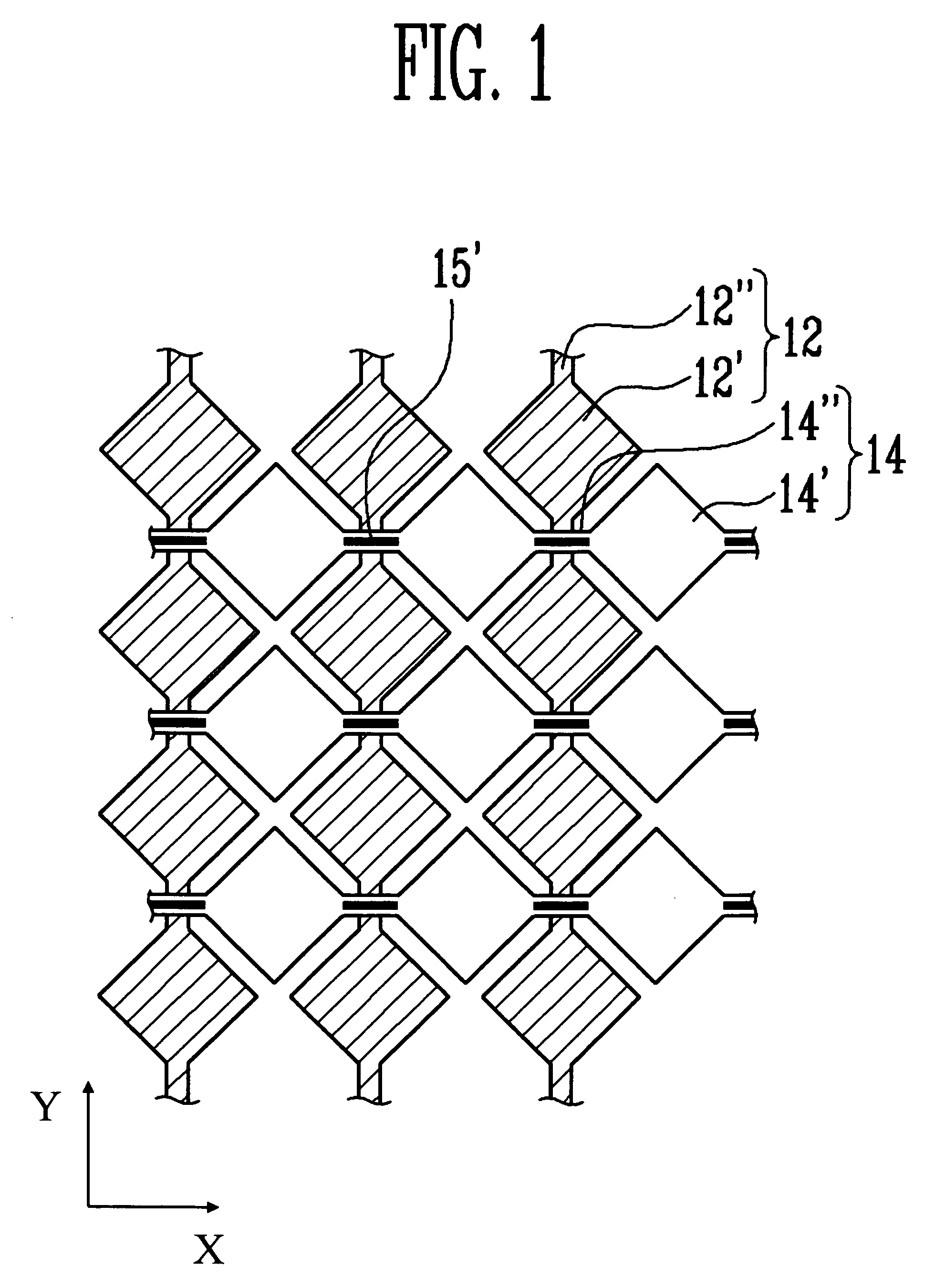
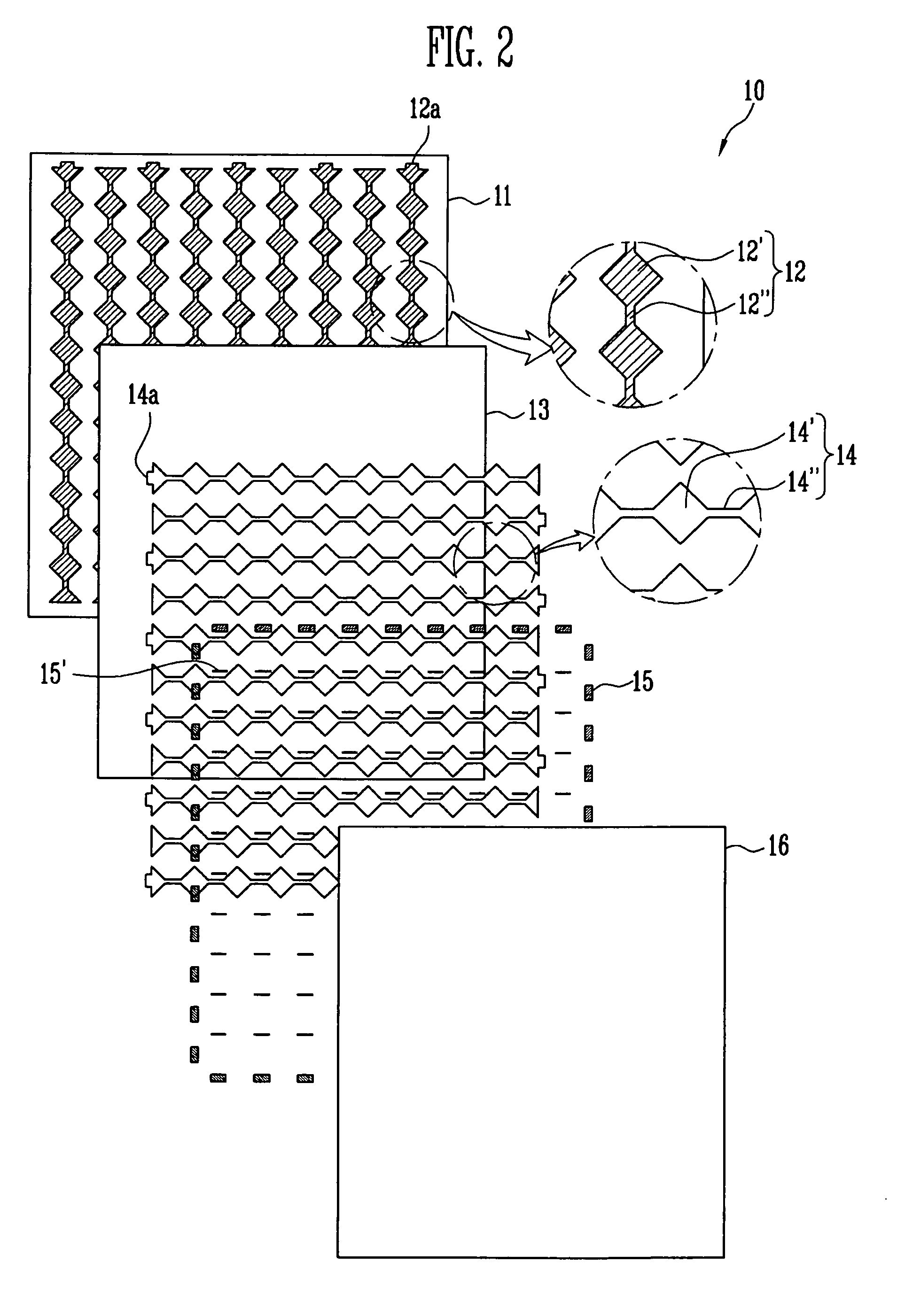
[0024]In the following detailed description, only certain exemplary embodiments of the present invention have been shown and described, simply by way of illustration. As those skilled in the art would realize, the described embodiments may be modified in various different ways, all without departing from the spirit or scope of the present invention. Accordingly, the drawings and description are to be regarded as illustrative in nature and not restrictive. In addition, when an element is referred to as being “on” another element, it can be directly on the element or be indirectly on the element with one or more intervening elements interposed therebetween. Also, when an element is referred to as being “connected to” another element, it can be directly connected to the element or be indirectly connected to the element with one or more intervening elements interposed therebetween. Hereinafter, like reference numerals refer to like elements.

[0025]Hereinafter, exemplary embodiments accor...


PUM


Abstract

The touch screen panel of the present invention includes first sensing patterns formed on a transparent substrate, a first insulating film formed on the first sensing patterns, second sensing patterns formed on the first insulating film, a plurality of metal patterns disposed on edge regions of the first and second sensing patterns, and a plurality of auxiliary metal patterns formed in the same layer as the metal patterns. Each of the first and second sensing patterns has sensing cells and coupling lines. Each of the coupling lines connects two of the sensing cells. Each of the metal patterns is coupled to the first sensing pattern or to the second sensing pattern, and each of the auxiliary metal patterns being formed on one of the first coupling lines or on one of the second coupling lines.

Description

CLAIM OF PRIORITY[0001]This application makes reference to, incorporates the same herein, and claims all benefits accruing under 35 U.S.C. §119 from an application earlier filed in the Korean Intellectual Property Office on 16 Jan. 2009 and there duly assigned Serial No. 10-2009-0003642.BACKGROUND OF THE INVENTION[0002]1. Field of the Invention[0003]The present invention relates to a touch screen panel, and more particularly, to a touch screen panel that minimizes resistance of an intersection portion of first and second sensing patterns.[0004]2. Description of the Related Art[0005]A touch screen panel is an input device through which a user can input his or her instruction by selecting an instructed content displayed on a screen such as an image display device, etc. using a human's finger or an object.[0006]To this end, the touch screen panel is provided on the front face of the image display device to convert a contact position, which the human's finger or object directly contacts...

Claims


Application Information

Patent Timeline
Patent Type & Authority Applications(United States)
IPC IPC(8): G06F3/041
CPCG06F3/044G06F2203/04111G06F3/0445G06F3/0446G06F2203/04103G06F2203/04104G06F2203/04107G06F3/0412
Inventor JEONG, HWAN-HEEJUNG, TAE-HYEOGKANG, SUNG-KUPARK, JUNG-MOKLEE, CHOON-HYOPKIM, SHAWNKIM, SANG-KOOK
Owner SAMSUNG DISPLAY CO LTD
Why Eureka
Try Eureka