Electromagnetic interference shielding structure including carbon nanotube or nanofiber films and methods

Active Publication Date: 2010-07-29
FLORIDA STATE UNIV RES FOUND INC
View PDF21 Cites 84 Cited by
  • Summary
  • Abstract
  • Description
  • Claims
  • Application Information

AI Technical Summary

Benefits of technology

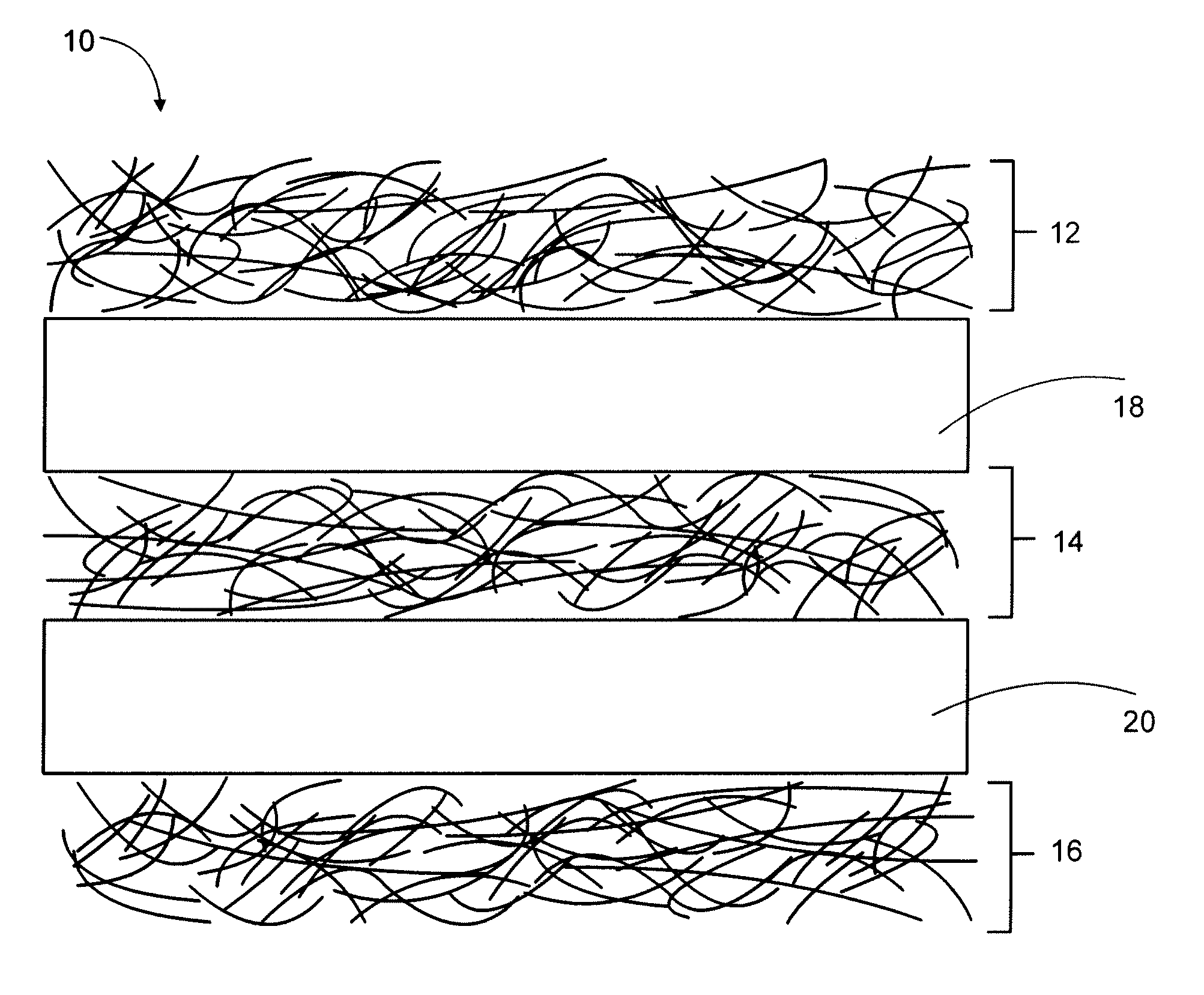
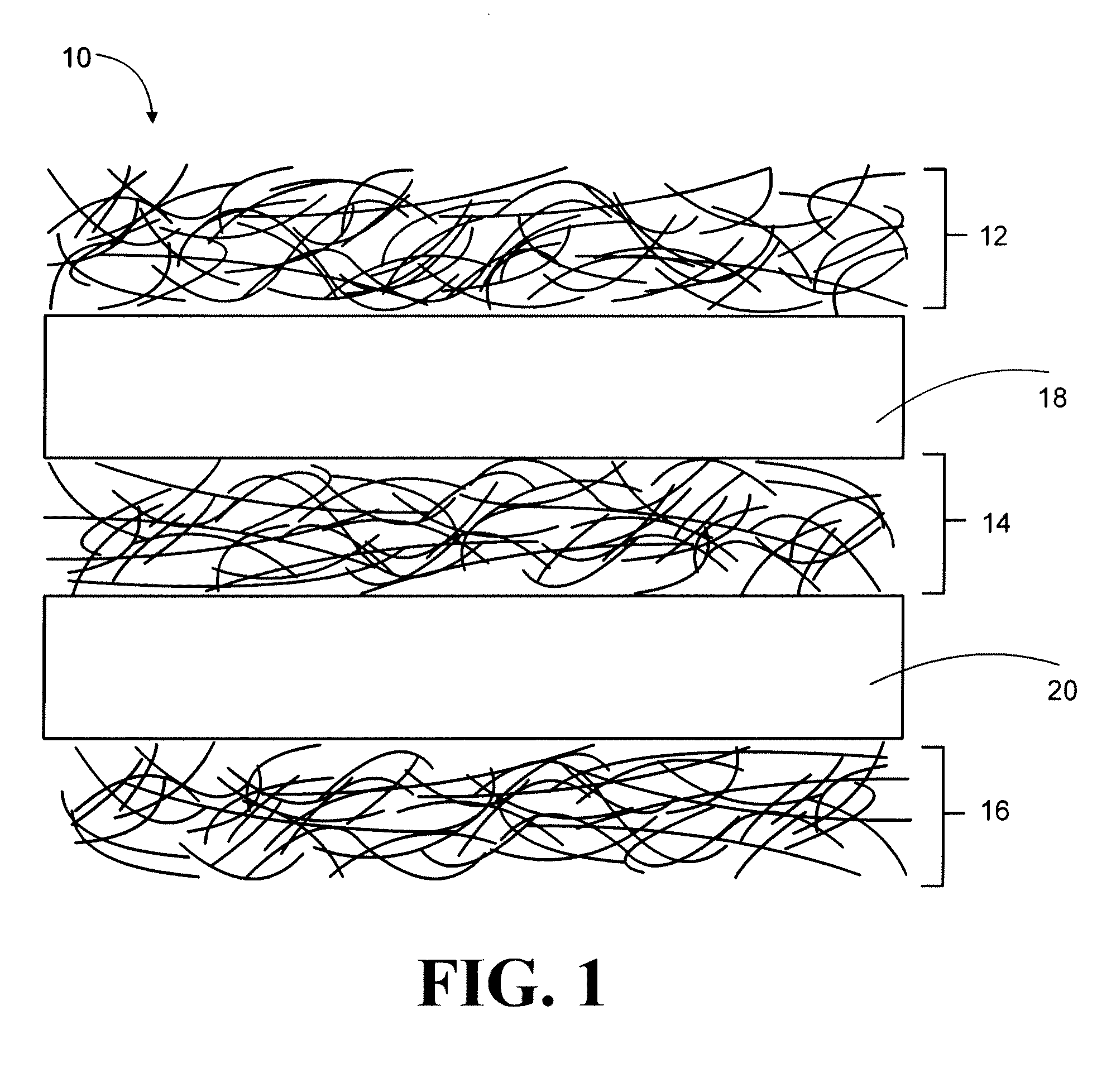
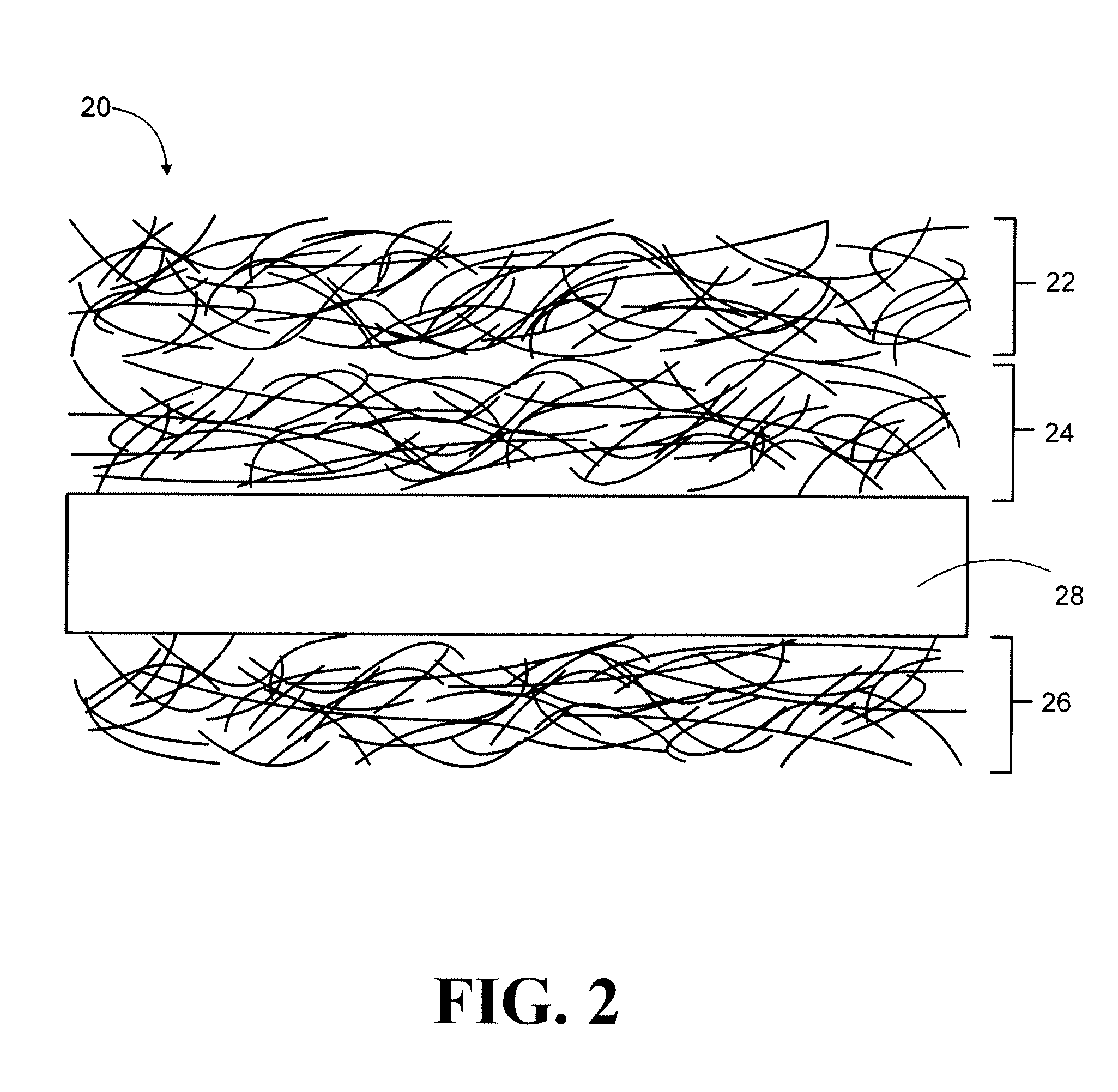
[0018]In yet another aspect, a method for shielding an electrical circuit from electromagnetic interference is provided. The method comprises positioning a composite material between the electrical circuit and an electromagnetic energy transmission source. The composite material comprises at least two electrically conductive nanoscale fiber films overlyi

Problems solved by technology

Metal serves as an effective shielding material because of its high conductivity, but metal adds significant weight and corrosion issues.
However, such methods can fail to achieve high nanotube loading and high conductivity in composites, which would be desirable for EMI shielding

Method used


Image

  • Electromagnetic interference shielding structure including carbon nanotube or nanofiber films and methods
  • Electromagnetic interference shielding structure including carbon nanotube or nanofiber films and methods
  • Electromagnetic interference shielding structure including carbon nanotube or nanofiber films and methods

Examples


example 1

[0096]Inclusion of BP with a thickness of 10-15 μm in a composite with low density polyethylene (LDPE) film (from McMaster, 500 microns in thickness) provided EMI shielding performance, in addition to flexibility and suitable mechanical properties for handling. The polymer film and BP layers were hot pressed at slightly above the melting temperature of the polymer film (149° C.). Test panels (6″×6″) were made. The total thickness of the panels (0.5 mm) was primarily due to the LDPE thickness, since the BP was very thin.

[0097]FIG. 3 shows the scanning electron microscope image of a SWNT / MWNT mixed BP. FIG. 4A shows the SEM image of the fracture surface of a BP composite made by the hot press process and including a polymer film inserted between two BP layers. The BP may be seen on the edge of the panel and LDPE covered the BP layers. FIG. 4B shows the enlarged image of the BP region in the composite. The LDPE polymer around the carbon nanotube was seen and filled some voids in the BP...

example 2

[0101]In this example, a vacuum bagging process was used to make BP composites for EMI shielding tests. Multiple layers of BP with EPON862 resin and polymethacrylimide (PMI) foam were used to compare their multiple reflection contributions to the EMI SE of the resulting composite structures. A modified MIL-STD-285 was adopted for broadband frequency range and a relatively large test panel size (7″×7″) was used. Those results were compared to a theoretical estimation including absorption, reflection, and multiple reflections.

[0102]The nanotube materials used were BuckyPearls™, purified single-walled nanotubes (SWNTs) from Carbon Nanotechnologies Inc (CNI). The SWNT BPs were produced using a filtration process. An aqueous suspension of nanotubes was prepared by a multiple-step dispersion procedure using sonication and a surfactant (Triton X-10, from Fisher Scientific). The suspension was filtered through a 0.45 μm filter in order to produce randomly dispersed BP sheets.

[0103]BPs havin...

example 3

[0116]The EMI SE of BP based composite structures with different conductivities and the effect of multiple layers was studied. A vacuum bagging process was used to make BP composites for EMI shielding tests. The nanotube materials used were BuckyPearls™, purified SWNT (Unidym Inc., TX) made by a Hipco process. In order to reduce the cost and increase the structural integrity of the application, multi-walled carbon nanotubes (MWNTs, Sigma-Aldrich) and vapor-grown carbon nanofiber (VGCNF, Applied Science Inc.) were mixed together with SWNTs in some samples.

[0117]The BPs were produced using the filtration process described in Example 2. SWNT BP having a 15 μm thickness and a basis weight of 21.5 g / m2 were produced because of the BP's high electrical conductivity, extremely lightweight structure, and nanoscale porosity. In the case of SWNT / MWNT mixed BP, MWNT or CNF was mixed with SWNT by weight ratio of 1:3 in the suspension. The typical thickness was 20-25 μm, which was thicker than t...


PUM


Abstract

A composite material for electromagnetic interference shielding is provided. The composite material comprises a stack including at least two electrically conductive nanoscale fiber films, which are spaced apart from one another by at least one insulating gap positioned between the at least two nanoscale fiber films. The stack is effective to provide a substantial multiple internal reflection effect. An electromagnetic interference shielded apparatus and a method for shielding an electrical circuit from electromagnetic interference is provided

Description

CROSS-REFERENCE TO RELATED APPLICATIONS[0001]This application claims benefit of U.S. Provisional Application No. 61 / 147,939, filed Jan. 28, 2009, which is incorporated herein by reference.STATEMENT REGARDING FEDERALLY SPONSORED RESEARCH OR DEVELOPMENT[0002]This invention was made with U.S. government support under Contract No. FA9550-05-1-0271 awarded by the Air Force Office of Scientific Research. The U.S. government has certain rights in the invention.BACKGROUND OF INVENTION[0003]This invention relates generally to nanoscale fibers, and more particularly to electromagnetic interference (EMI) shielding structures comprising nanoscale fibers.[0004]Due to the growing need for more powerful and compact electronic products, EMI is becoming a more significant factor in commercial and military applications. The EMI shielding of electronic devices and / or radiation sources may be a consideration in the reliable operation of devices, and possibly in preventing human health risks.[0005]Thin ...

Claims


Application Information

Patent Timeline
IPC IPC(8): H05K9/00H01B1/00H01B1/04
CPCH01B1/04H05K9/009Y10S977/832H05K9/0088B82Y30/00
Inventor LIANG, ZHIYONGWANG, BENZHANG, CHUNPARK, JIN GYU
Owner FLORIDA STATE UNIV RES FOUND INC
Why Eureka
Try Eureka