
Light Emitting Diode Unit, Display Apparatus Having the Same and Manufacturing Method of the Same

a technology display apparatuses, which is applied in the direction of electrical apparatus, semiconductor/solid-state device manufacturing, and semiconductor devices. it can solve the problems of color reproducibility degradation of light emitting diodes, reduce or prevent deterioration of quantum dots, and prolong the life of led units. , the effect of high degree of color reproduction

Inactive Publication Date: 2010-08-05
SAMSUNG DISPLAY CO LTD
View PDF8 Cites 139 Cited by
  • Summary
  • Abstract
  • Description
  • Claims
  • Application Information

AI Technical Summary

Benefits of technology

[0009]Exemplary embodiments of the present invention provide for an LED unit with enhanced color reproduction and an extended lifespan.
[0010]Exemplary embodiments of the present invention provide a display apparatus having enhanced color reproduction and an extended lifespan by using the LED unit as a light source.
[0025]As described above, the present invention can provide an LED unit having a relatively high degree of color reproduction. The LED unit is provided with a buffer layer that diffuses light emitted from the LED and accordingly, deterioration of the quantum dots can be reduced or prevented. Thus, the color reproduction of LED unit can be maintained and the lifespan of the LED unit can be extended.
[0026]Further, in using the LED unit within a display apparatus, the display apparatus may have a relatively high degree of color reproduction and a long lifespan.
[0027]Further, the LED unit can be effectively manufactured through a simple process.

Problems solved by technology

The full-width half-maximum of light emitted from red fluorescent material and the green fluorescent material is relatively wide, so that the color reproducibility of the light emitting diode unit is deteriorated.

Method used


Image

  • Light Emitting Diode Unit, Display Apparatus Having the Same and Manufacturing Method of the Same
  • Light Emitting Diode Unit, Display Apparatus Having the Same and Manufacturing Method of the Same
  • Light Emitting Diode Unit, Display Apparatus Having the Same and Manufacturing Method of the Same

Examples


Embodiment Construction

[0042]Hereinafter, exemplary embodiments of a display apparatus will be explained in detail with reference to the accompanying drawings. However, the scope of the present invention is not limited to such embodiments and the present invention may be realized in various forms. It should be understood that the figures may not be drawn to scale. Also, the same reference numerals may be used to designate the same elements throughout the drawings.

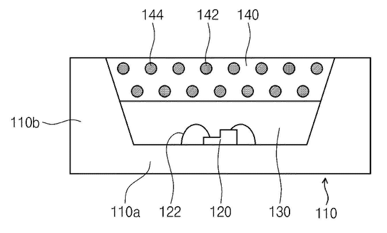
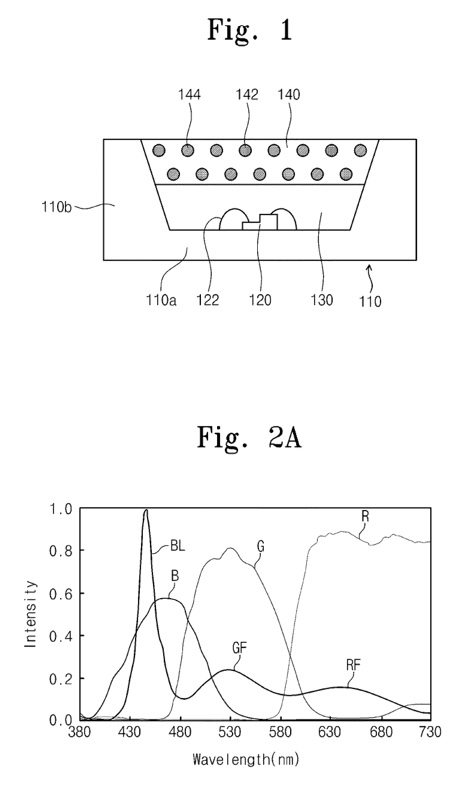
[0043]FIG. 1 is a sectional view illustrating an LED unit according to an exemplary embodiment of the present invention.

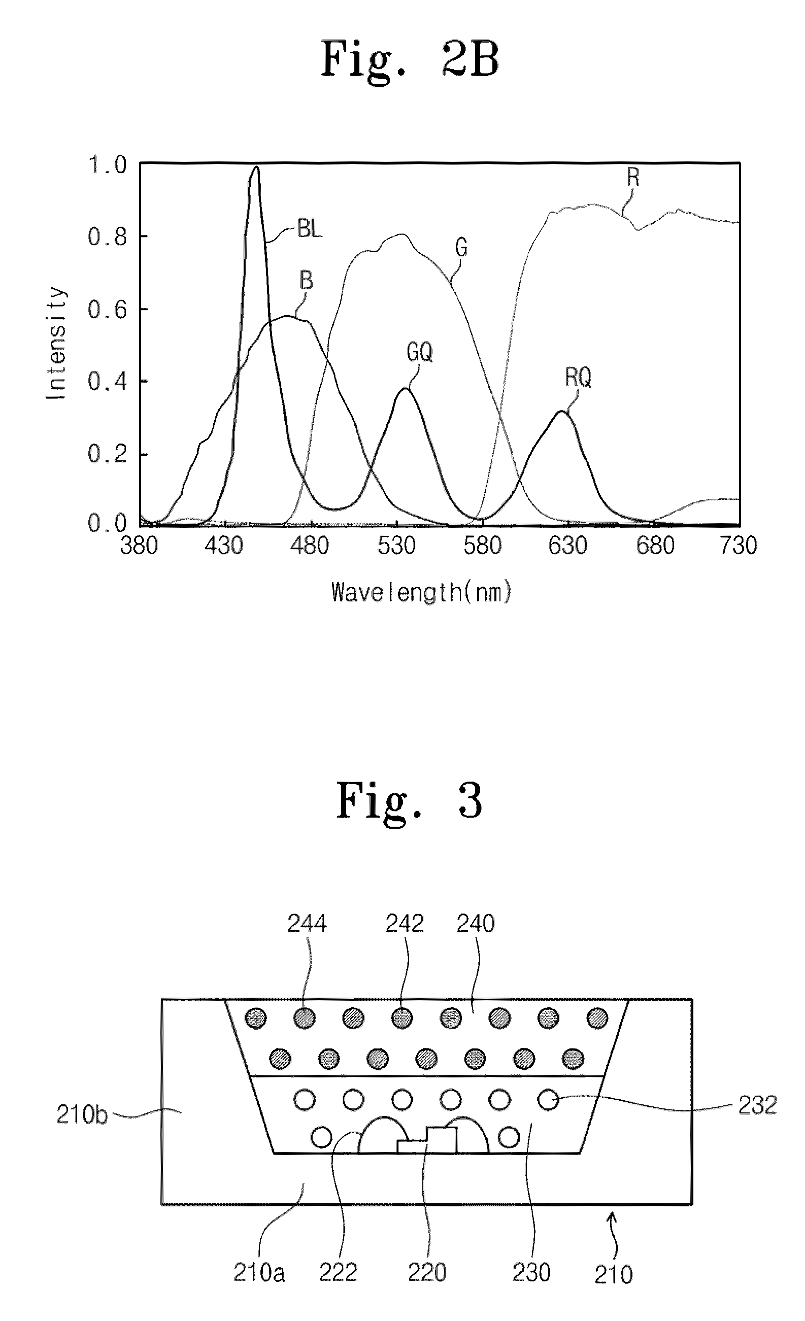
[0044]Referring to FIG. 1, the LED unit according to an exemplary embodiment of the present embodiment includes at least one LED 120 that emits light, a buffer layer 130 on the LED 120, and a quantum dot layer 140 on the buffer layer 130.

[0045]The LED 120, the buffer layer 130 and the quantum dot layer 140 are accommodated in a housing 110. The housing 110 has an internal space to receive the LED 120 thereon, the buffer layer 13...


PUM


Abstract

Disclosed are a light emitting diode unit, a display apparatus having the same, and a method of manufacturing the same. The light emitting diode unit includes at least one light emitting diode, a quantum dot layer, and a buffer layer. The light emitting diode emits first light. The quantum dot layer is provided on the light emitting diode and includes a plurality of quantum dots that absorb the first light to emit second light having a wavelength different from a wavelength of the first light. The buffer layer is interposed between the light emitting diode and the quantum dot layer and separates the light emitting diode from the quantum dot layer. The buffer layer includes a scattering agent which is dispersed in resin to diffuse the light emitted from the light emitting diode.

Description

CROSS-REFERENCE TO RELATED APPLICATION[0001]This application claims priority to Korean Patent Application No. 10-2009-0007946 filed on Feb. 02, 2009, the contents of which are herein incorporated by reference in their entirety.BACKGROUND OF THE INVENTION[0002]1. Technical Field[0003]The present invention relates to a light emitting diode unit, and more particularly, the present invention relates to a light emitting diode unit, a display apparatus having the light emitting diode unit, and a method of manufacturing the light emitting diode unit.[0004]2. Discussion of the Related Art[0005]A light emitting diode (LED) is a form of solid-state light source having a structure of a p-n junction. In the light emitting diode, energy of electrons is converted into light that is emitted. Electrons and holes, which are injected into the semiconductor from electrodes, are recombined in a region adjacent to the p-n junction when the energy exceeds a band gap (EG) of the p-n junction. During the r...

Claims


Application Information

Patent Timeline
IPC IPC(8): H01L33/00
CPCH01L33/507H01L2933/0091H01L2224/49107H01L2224/48091H01L2924/00014H01L2224/45139H01L2924/00011H01L2924/00H01L2924/01049H01L2924/01039H01L2224/45015H01L2924/207
Inventor BYUN, JINSEOB
Owner SAMSUNG DISPLAY CO LTD
Learn More