Semiconductor pressure sensor and manufacturing method thereof

a technology of semiconductors and sensors, applied in the direction of fluid pressure measurement, fluid pressure measurement by electric/magnetic elements, instruments, etc., can solve the problem of difficult accurate temperature compensation, and achieve the effect of removing the change in resistance value and high-precision temperature compensation

Inactive Publication Date: 2010-09-02
MITSUBISHI ELECTRIC CORP
View PDF4 Cites 3 Cited by
  • Summary
  • Abstract
  • Description
  • Claims
  • Application Information

AI Technical Summary

Benefits of technology

[0012]According to the semiconductor pressure sensor of the present invention, the first and second diaphragms have mutually identical or symmetrical structures, and the first and second gauge resistances have mutually identical or symmetrical structures. Therefore, it becomes possible to remove the change in re...

Problems solved by technology

In the strain sensor described in Japanese Patent Laying-Open No. 60-259922, the temperature-sensitive resistor is simply provided separate...

Method used


Image

  • Semiconductor pressure sensor and manufacturing method thereof
  • Semiconductor pressure sensor and manufacturing method thereof
  • Semiconductor pressure sensor and manufacturing method thereof

Examples


embodiment 1

[0025]First, a structure of the semiconductor pressure sensor in accordance with Embodiment 1 of the present invention will be described.

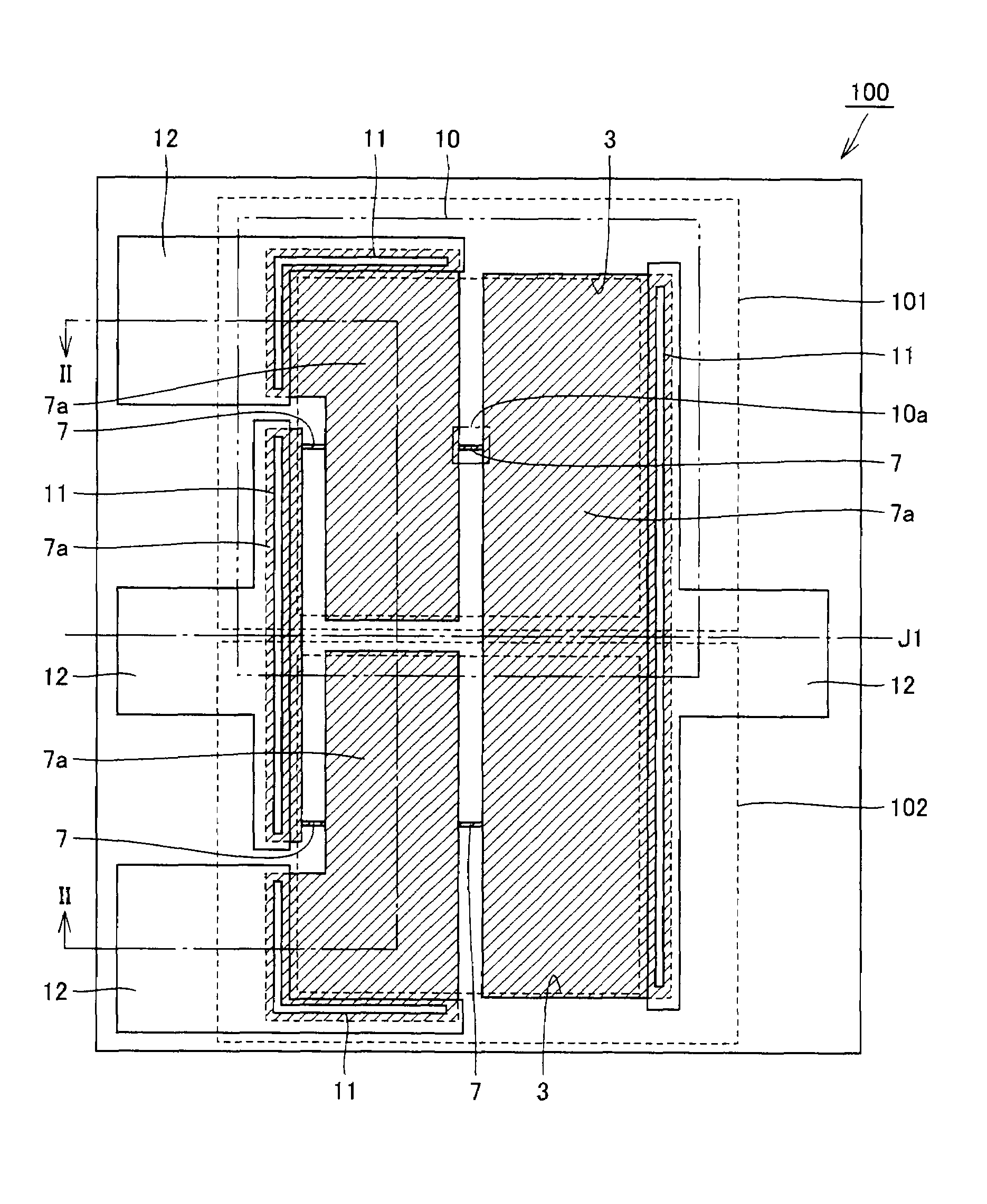
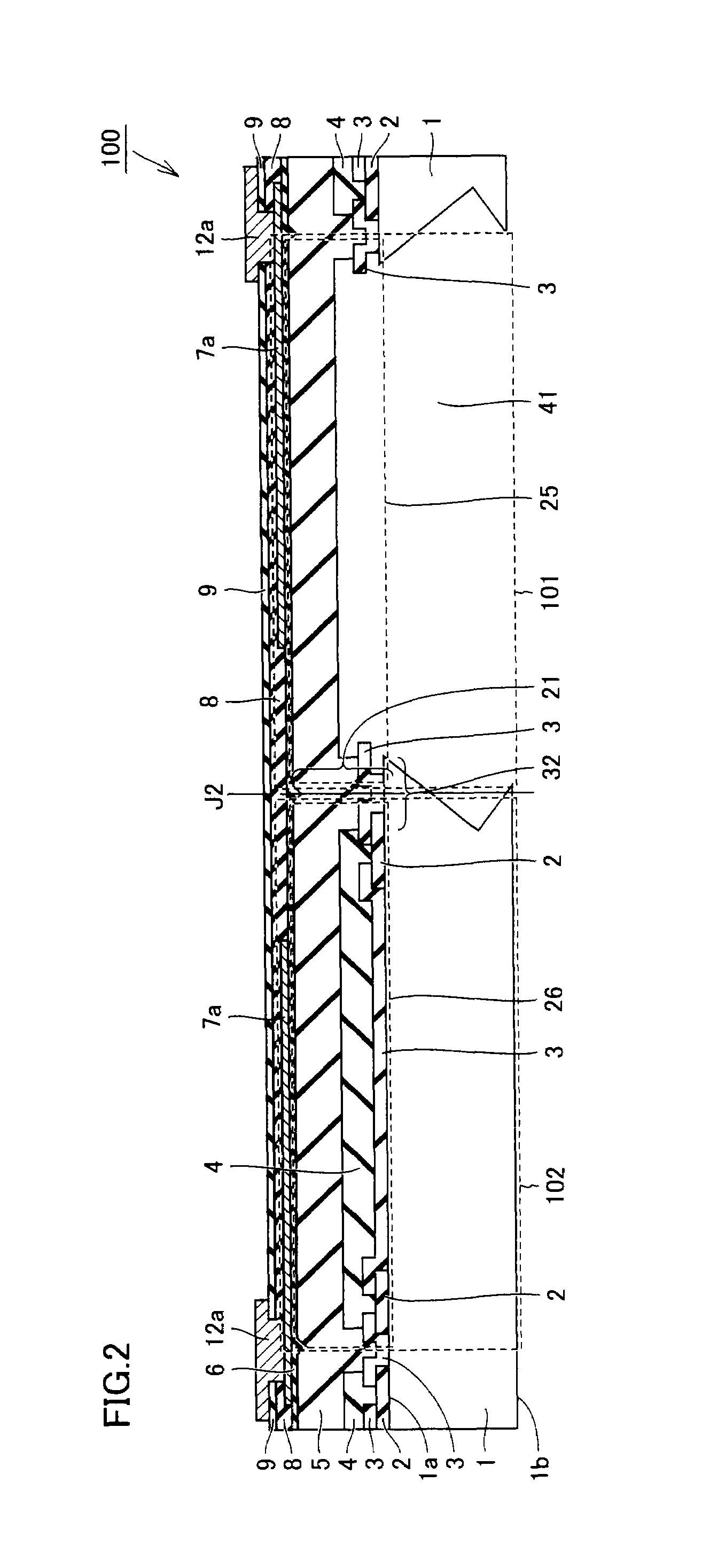
[0026]Referring to FIGS. 1 and 2, a semiconductor pressure sensor 100 mainly has an active gauge resistance forming portion 101 and a dummy gauge resistance forming portion 102 for temperature compensation. Active gauge resistance forming portion 101 and dummy gauge resistance forming portion 102 for temperature compensation are connected by a polycrystalline silicon (hereinafter referred to as “polysilicon”) interconnection 7a. In active gauge resistance forming portion 101 shown in FIG. 1, a diaphragm etching mask 10 and a diaphragm bottom surface 10a are drawn, for convenience of later description of the manufacturing method.

[0027]Active gauge resistance forming portion 101 mainly has a silicon substrate (substrate) 1, a first diaphragm 25, a gauge resistance 7, and an aluminum pad 12.

[0028]On a first main surface 1a of silicon substrate 1, a fi...

embodiment 2

[0078]Embodiment 2 of the present invention differs from Embodiment 1 mainly in the manner of etching silicon substrate 1.

[0079]Referring to FIG. 9, as compared with Embodiment 1, diaphragm etching mask 10 has an elongate shape along the longitudinal direction of gauge resistance 7 in the plan view. Further, diaphragm bottom surface 10a has a shape of a parallelogram in the plan view.

[0080]Referring to FIG. 10, through hole 41 formed in silicon substrate 1 to extend from the second main surface 1b to the first main surface 1a, extends substantially vertically to a middle portion between the second main surface 1b and the first main surface 1a from the second main surface 1b. Through hole 41 is formed to be gradually wider from the middle portion between the second main surface 1b and the first main surface 1a to the first main surface 1a.

[0081]Referring to FIG. 11, a silicon substrate 1 of which second main surface 1b has crystal orientation of (110) is used. Thereafter, through th...

embodiment 3

[0085]Embodiment 3 of the present invention differs from Embodiment 1 mainly in gauge resistance 7 and polysilicon interconnection 7a.

[0086]Referring to FIG. 14, a plurality of dummy polysilicon patterns (dummy patterns) 7b are formed in a direction intersecting longitudinal direction of gauge resistance 7. Dummy polysilicon patterns 7b are arranged to have the same width and space as the width and space of gauge resistance 7 in a plan view.

[0087]Referring to FIG. 15, dummy polysilicon pattern 7b formed of the same polysilicon film as polysilicon interconnection 7a is formed on the third insulating film 6. Further, gauge resistance 7 is formed next to dummy polysilicon pattern 7b.

[0088]As shown in FIG. 15, dummy polysilicon 7b is formed on third insulating film 6. Dummy polysilicon pattern 7b is formed, by way of example, by introducing an impurity such as B to an undoped polysilicon film.

[0089]Except for the points described above, the structure and manufacturing method in accord...


PUM


Abstract

A semiconductor pressure sensor includes a silicon substrate, an active gauge resistance forming portion having a first diaphragm and a first gauge resistance formed on the silicon substrate, and a dummy gauge resistance forming portion for temperature compensation having a second diaphragm and a second gauge resistance, formed on the substrate. The first diaphragm of the active gauge resistance forming portion and the second diaphragm of the dummy gauge resistance forming portion for temperature compensation are formed of a common polysilicon film. The polysilicon film has an anchor portion to be connected to the substrate. The first and second diaphragms have mutually identical or symmetrical structures and the first and second gauges have mutually identical or symmetrical structures. Accordingly, a semiconductor pressure sensor capable of highly accurate temperature compensation and manufacturing method thereof can be provided.

Description

BACKGROUND OF THE INVENTION[0001]1. Field of the Invention[0002]The present invention relates to a semiconductor pressure sensor and manufacturing method thereof and, more specifically, to a semiconductor pressure sensor capable of temperature compensation and manufacturing method thereof.[0003]2. Description of the Background Art[0004]In a conventional semiconductor pressure sensor, a diffusion resistance that will be a gauge resistance, is formed in a silicon substrate. A plurality of gauge resistances are bridge-connected by diffusion interconnections of low resistance. A diaphragm is formed by etching from a rear surface of the silicon substrate. Gauge resistances are arranged at an edge portion of the diaphragm.[0005]By way of example, Japanese Utility Model Laying-Open No. 63-178353 describes a semiconductor pressure sensor having a diaphragm formed of an oxide film, a polysilicon substrate, an oxide film and a gauge, formed on a silicon substrate with a through hole.[0006]Fur...

Claims


Application Information

Patent Timeline
IPC IPC(8): G01L9/02G01L19/04H01L21/02
CPCG01L9/0042G01L9/065G01L9/0055G01L9/04G01L9/00H01L29/84G01L1/20
Inventor SATO, KIMITOSHI
Owner MITSUBISHI ELECTRIC CORP
Why Eureka
Try Eureka