Demodulator Capable of Compensating Offset Voltage of RF Signal and Method Thereof

Active Publication Date: 2010-09-02
3A LOGICS
View PDF17 Cites 2 Cited by
  • Summary
  • Abstract
  • Description
  • Claims
  • Application Information

AI Technical Summary

Benefits of technology

[0007]In a demodulator and a method of compensating for an offset voltage included in an RF signal according to the present invention, distortion and a signal-to-no

Problems solved by technology

Consequently, reception sensiti

Method used


Image

  • Demodulator Capable of Compensating Offset Voltage of RF Signal and Method Thereof
  • Demodulator Capable of Compensating Offset Voltage of RF Signal and Method Thereof
  • Demodulator Capable of Compensating Offset Voltage of RF Signal and Method Thereof

Examples


Embodiment Construction

Technical Problem

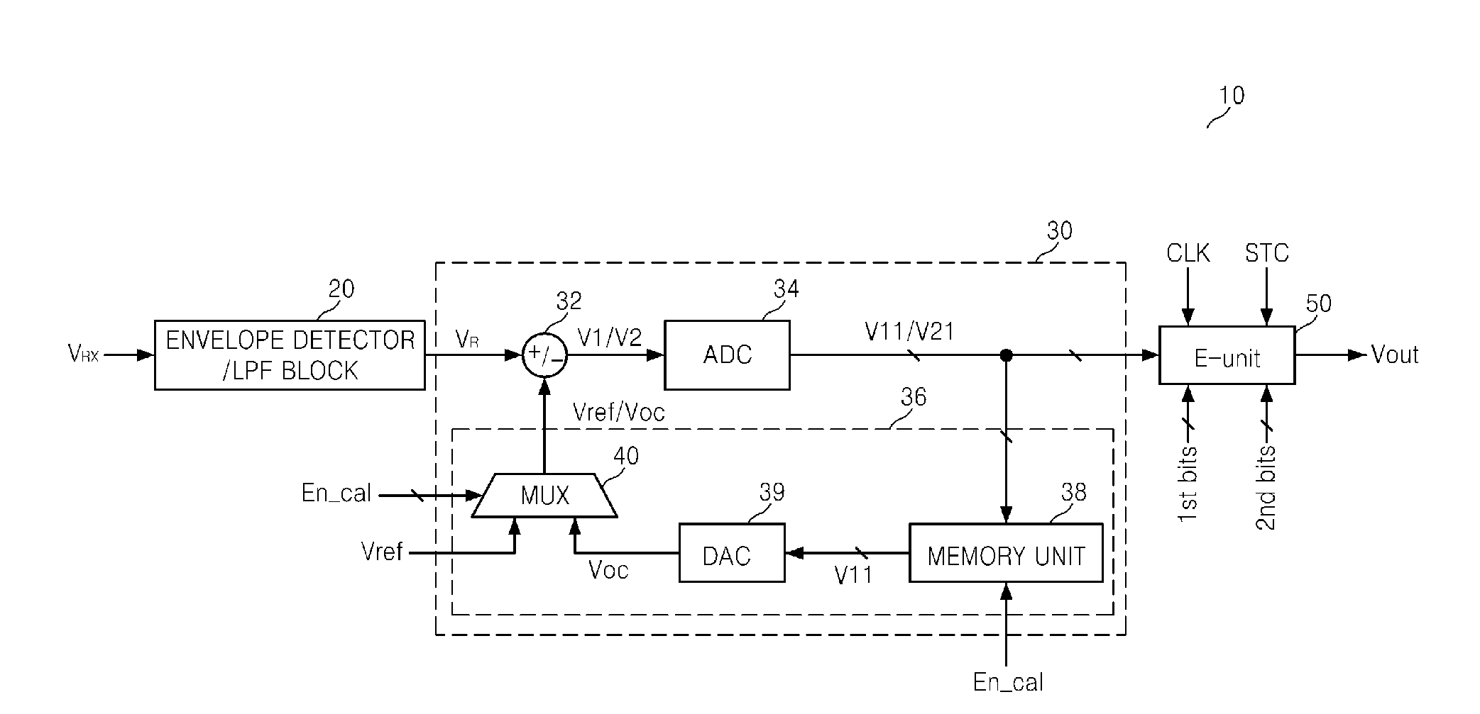
[0006]The present invention provides a demodulator that includes an offset voltage compensation voltage generation block and is capable of compensating for an offset voltage of an RF signal received from an RF tag, and a method of compensating for the offset voltage of the RF signal.

Advantageous Effects

[0007]In a demodulator and a method of compensating for an offset voltage included in an RF signal according to the present invention, distortion and a signal-to-noise ratio (SNR) of the RF signal are reduced by compensating for the offset voltage of the RF signal. Thus, reception sensitivity of an RF receiver can be improved.

DESCRIPTION OF THE DRAWINGS

[0008]The above and other features and advantages of the present invention will become more apparent by describing in detail exemplary embodiments thereof with reference to the attached drawings in which:

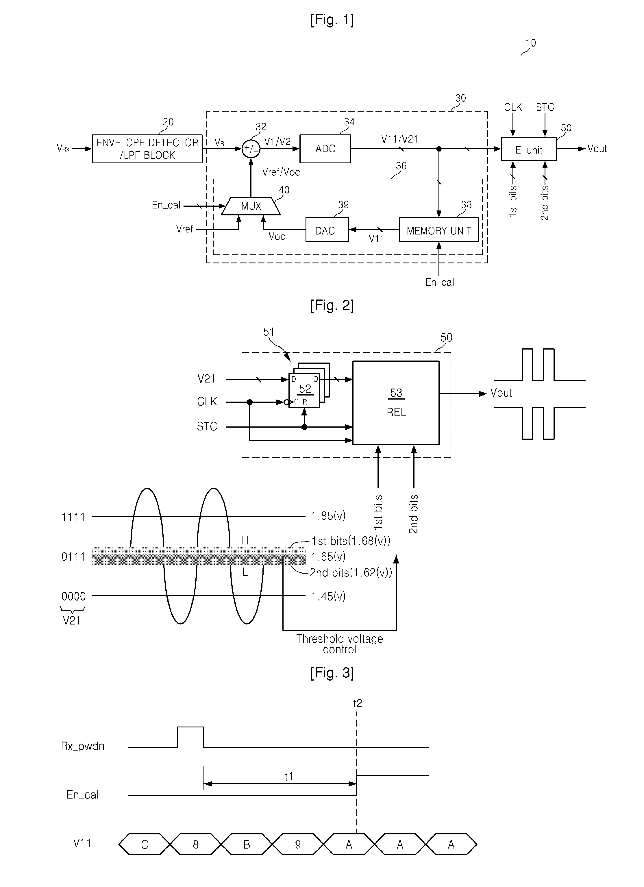
[0009]FIG. 1 is a function block diagram of a demodulator according to an embodiment of the present invention;
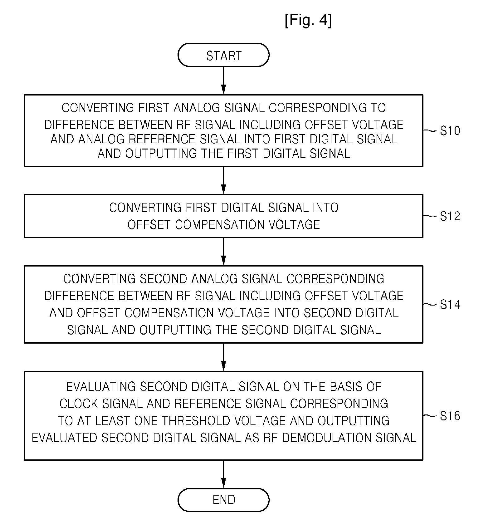
[0010]F...


PUM


Abstract

A demodulator capable of compensating for an offset voltage of a radio frequency (RF) signal, and a method of compensating for the offset voltage of the RF signal are provided. The demodulator includes an analog-to-digital conversion (ADC) unit for converting a first analog signal corresponding to a difference between the RF signal comprising the offset voltage and an analog reference signal into a first digital signal, and a compensation voltage generation unit for converting the first digital signal into an offset compensation voltage. The ADC unit converts a second analog signal corresponding to a difference between the RF signal comprising the offset voltage and the offset compensation voltage into a second digital signal. Accordingly, the offset voltage included in the RF signal is compensated for, and thus distortion and a signal-to-noise ratio (SNR) of the RF signal are reduced. This leads to an improvement of the reception sensitivity of an RF receiver.

Description

TECHNICAL FIELD[0001]An embodiment of the present invention relates to a demodulator, and more particularly, to a demodulator capable of compensating for an offset voltage of a radio frequency (RF) signal and a method of compensating for an offset voltage of an RF signal.BACKGROUND ART[0002]Typically, radio frequency identification (RFID) systems may be classified into an inductively coupled system and an electromagnetic wave system according to wireless connecting methods. The inductively coupled system is used in RFID systems for short distances (i.e., 1 m or less), and enables an RF signal receiver (for example, a reader) and an RF signal transmitter (for example, an RF tag) to perform wireless communications by using coil antennas.[0003]An RF tag in the inductively coupled system is almost manually operated. In other words, all of energies required for an IC chip of the RF tag to operate are supplied by a reader. Accordingly, an antenna coil of the reader generates a strong magn...

Claims


Application Information

Patent Timeline
IPC IPC(8): H03M1/00
CPCH04B1/30H04B1/10H04B1/12
Inventor KIM, SUNG WANLEE, PYEONG HANCHUN, SUNG HUN
Owner 3A LOGICS
Why Eureka
Try Eureka