Solid-state image pickup apparatus, method of manufacturing the same, and image pickup apparatus

Active Publication Date: 2010-09-16
SONY SEMICON SOLUTIONS CORP
View PDF4 Cites 45 Cited by
  • Summary
  • Abstract
  • Description
  • Claims
  • Application Information

AI Technical Summary

Benefits of technology

[0023]In the image pickup apparatus according to the embodiment of the present invention, it is possible to adjust the spectral balance in the difference of spread angles of light from the waveguide exit end due to the wavelengths of the colors.
[0024]The solid-state image pickup apparatus of the present invention can adjust the spectral balance. Thus, an image synthesis margin can be obtained in making an adjustment for an image of a more natural color, and a color correction can be easily performed, with the result that the advantage of obtaining an image excellent in color reproducing performance can be provided.
[0025]By the method of manufacturing a solid-state image pickup apparatus of

Problems solved by technology

There is a problem of deterioration of the spectral

Method used


Image

  • Solid-state image pickup apparatus, method of manufacturing the same, and image pickup apparatus
  • Solid-state image pickup apparatus, method of manufacturing the same, and image pickup apparatus
  • Solid-state image pickup apparatus, method of manufacturing the same, and image pickup apparatus

Examples


first embodiment

1. First Embodiment

(First Example of Structure of Solid-State Image Pickup Apparatus)

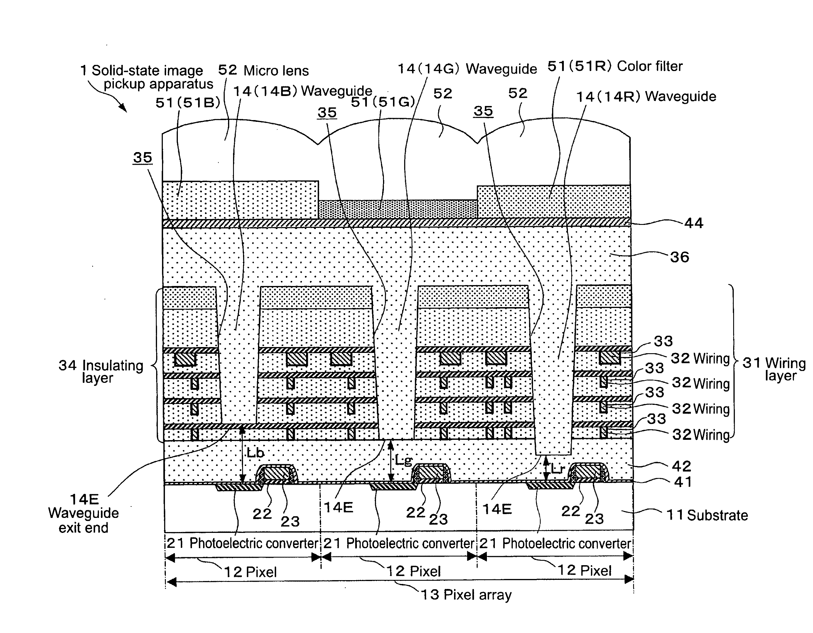
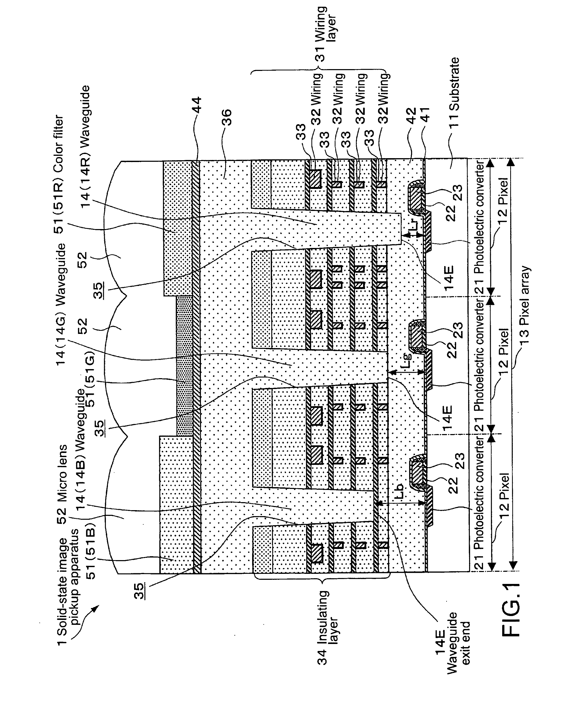
[0045]A first example of a structure of a solid-state image pickup apparatus according to a first embodiment of the present invention will be described with reference to a cross-sectional diagram of a schematic structure of FIG. 1.

[0046]As shown in FIG. 1, on a substrate 11, a pixel array portion 13 constituted of a plurality of pixels 12 each including a photoelectric converter 21 is provided. The photoelectric converter 21 converts incident light to an electrical signal. For the substrate 11, for example, a silicon substrate as a semiconductor substrate is used. The photoelectric converter 21 is formed of a photodiode, for example. Further on the substrate 11, a transfer gate electrode 23 is formed to be adjacent to the photoelectric converter 21 through a gate insulating film 22.

[0047]Further, on the substrate 11, a protection film 41 that covers the photoelectric converter 21, the transfer gate ...

second embodiment

2. Second Embodiment

(First Example of Method of Manufacturing Solid-State Image Pickup Apparatus)

[0121]Next, a description will be given on a first example of a method of manufacturing a solid-state image pickup apparatus according to a second embodiment of the present invention with reference to manufacture-process cross-sectional diagrams of FIGS. 9 to 11.

[0122]As shown in FIG. 9A, on the substrate 11, the pixel array portion 13 constituted of the plurality of pixels 12 each including the photoelectric converter 21 that converts the incident light into an electrical signal is formed. For the substrate 11, a silicon substrate is used as a semiconductor substrate, for example. The photoelectric converter 21 is formed of a photodiode, for example. Further, on the substrate 11, the transfer gate electrode 23 is formed to be adjacent to the photoelectric converter 21 through the gate insulating film 22. In addition, a pixel transistor, a peripheral circuit, and the like (not shown) are...

third embodiment

3. Third Embodiment

(Example of Structure of Image Pickup Apparatus)

[0212]A description will be given on an example of a structure of an image pickup apparatus according to a third embodiment of the present invention with reference to a block diagram of FIG. 16. In the image pickup apparatus, the solid-state image pickup apparatus according to the embodiments of the present invention is used.

[0213]As shown in FIG. 16, an image pickup apparatus 200 includes a solid-state image pickup apparatus (not shown) in an image pickup portion 201. On a light-collecting side of the image pickup portion 201, a light-collecting optical portion 202 that forms an image is provided. Further, to the image pickup portion 201, connected is a signal processing portion 203 having a drive circuit that drives the image pickup portion 201 and a signal processing circuit that performs an image processing on a signal that has been subjected to the photoelectric conversion in the solid-state image pickup apparat...


PUM


Abstract

A solid-state image pickup apparatus includes a substrate, a wiring layer, and a waveguide. The substrate is provided with a pixel array portion constituted of a plurality of pixels each having a photoelectric converter that converts incident light into an electrical signal. The wiring layer includes a plurality of wirings and an insulating layer that covers the plurality of wirings that are laminated above the substrate. The waveguide guides light to each of the photoelectric converters of the plurality of pixels, the waveguide being formed in the wiring layer. The waveguide is formed to have a waveguide exit end from which light exits the waveguide so that a distance between the waveguide exit end and a surface of the photoelectric converter that receives light from the waveguide become shorter, as wavelengths of light guided by the waveguide are longer.

Description

CROSS-REFERENCE TO RELATED APPLICATION[0001]The present application claims priority from Japanese Patent Application No. JP 2009-058985 filed in the Japanese Patent Office on Mar. 12, 2009, the entire content of which is incorporated herein by reference.BACKGROUND OF THE INVENTION[0002]1. Field of the Invention[0003]The present invention relates to a solid-state image pickup apparatus, a method of manufacturing the same, and an image pickup apparatus.[0004]2. Description of the Related Art[0005]In response to the progress of the increase in number of pixels and the miniaturization of a pixel size, there has been proposed a technique of using a waveguide structure as a means for increasing a light collection efficiency of each pixel in a solid-state image sensor. In particular, in a CMOS image sensor, for forming a metal wiring on a light incident side of a photodiode, a waveguide structure, which guides incident light to a photodiode while confining the light and avoiding the metal ...

Claims


Application Information

Patent Timeline
IPC IPC(8): H01L27/146H01L31/0232H01L31/18H01L27/14H04N5/335H04N5/369H04N5/374H04N9/07
CPCH01L27/14621H01L27/14625H01L27/14627H01L27/14629H01L27/14645H01L27/14685H01L27/14636
Inventor HORIKOSHI, HIROSHIKIKUCHI, KOJIYAMAZAKI, TOMOHIRO
Owner SONY SEMICON SOLUTIONS CORP
Why Eureka
Try Eureka