

Solid-state imaging device and imaging apparatus
a solid-state imaging and imaging device technology, applied in the field of solid-state imaging devices and imaging apparatuses, can solve the problems of reducing the manufacturing yield of pixels, reducing the quality of burying in optical waveguides, and limiting the miniaturization of pixel having optical waveguides, so as to prevent the generation of loss due to invalid zones, the effect of reducing the area of light receiving units when miniaturizing pixels and reducing the area of the light receiving units
Active Publication Date: 2010-09-30
SONY SEMICON SOLUTIONS CORP
View PDF3 Cites 34 Cited by
- Summary
- Abstract
- Description
- Claims
- Application Information
AI Technical Summary
Benefits of technology
[0009]The formation of an optical waveguide includes the step of burying a material in the inside thereof. However, if a pixel is made finer, then the opening size of the optical waveguide is made smaller. It causes a decrease in quality of burying in the optical waveguide because of facilitated generation of an air bubble or the like in the manufacturing process. Thus, there is a limit in miniaturization of a pixel having an optical waveguide. Therefore, a decrease in quality of burying of the optical waveguide as described above leads to widely varied qualities of burying the optical waveguides in the respective pixels, resulting in a decrease in manufacturing yield of the pixels.
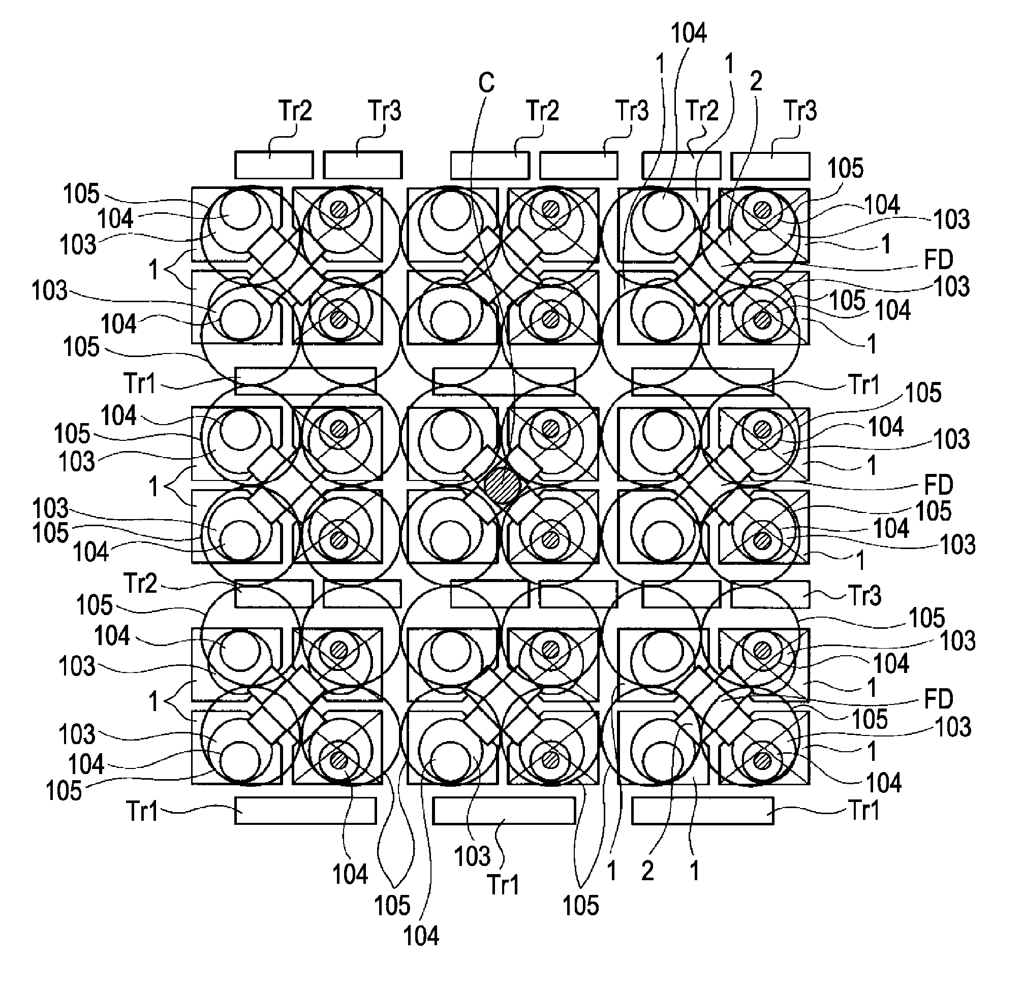
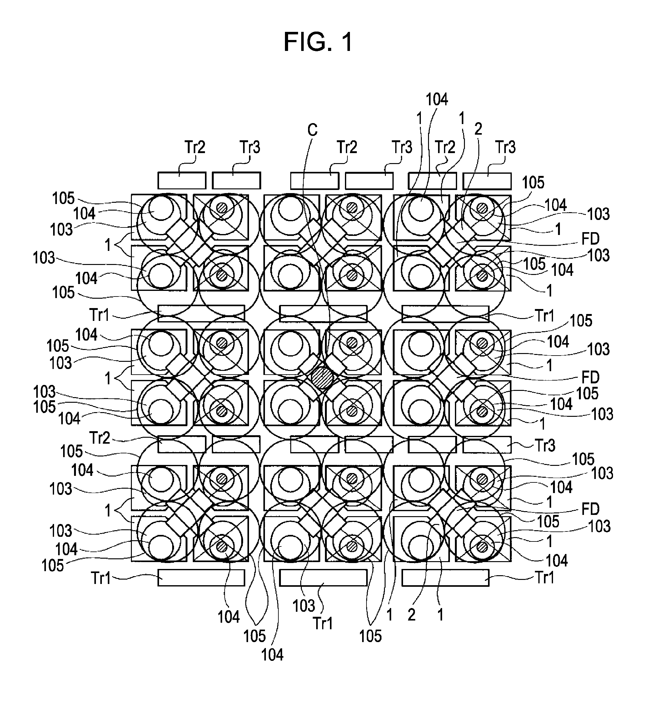
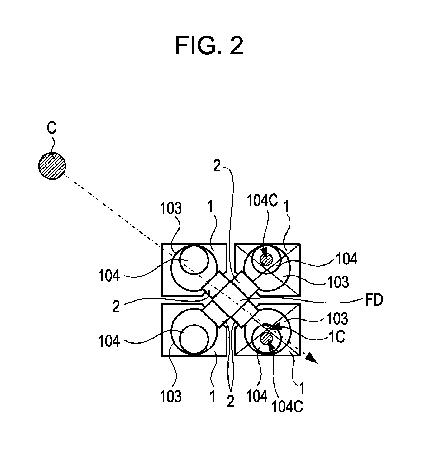
[0010]To avoid such disadvantages, there is an idea like the one described in Japanese Patent Laid Open No. 2006-303468 in which a solid-imaging device having an optical waveguide is designed so that two or more pixels share a transistor and a floating diffusion. The sharing of the transistor and the floating diffusion by two or more pixels can extend the surface area of the light receiving unit per pixel as compared with an unshared case. In other words, the reduction of the surface area of the light receiving unit can be diminished when the pixel is made finer. Thus, the reduction of the opening size of the optical waveguide can be also diminished.
Problems solved by technology
It causes a decrease in quality of burying in the optical waveguide because of facilitated generation of an air bubble or the like in the manufacturing process.
Thus, there is a limit in miniaturization of a pixel having an optical waveguide.
Therefore, a decrease in quality of burying of the optical waveguide as described above leads to widely varied qualities of burying the optical waveguides in the respective pixels, resulting in a decrease in manufacturing yield of the pixels.
Method used
View moreImage
Smart ImageViewing Examples

Examples
second embodiment
2. Second embodiment of solid-state imaging device;
3. Modified embodiment;
third embodiment
4. Third embodiment of solid-state imaging device;
fourth embodiment
5. Fourth embodiment of solid-state imaging device;
6. Modified embodiment; and
7. Embodiment of imaging apparatus.
Login to View More PUM
 Abstract
An imaging device includes a basic cell having two or more the pixels that share floating diffusion. The imaging device also includes a transistor shared by the two or more pixels in the basic cell and arranged on the outside of the two or more pixels. The imaging device further includes a light receiving unit connected to the floating diffusion shared by the pixels in the basic cell through a transfer gate. In the imaging device, on-chip lenses are arranged substantially at regular intervals. Also, an optical waveguide is formed so that the position thereof in the surface of the solid-state imaging device is located at a position shifted from the center of the light receiving unit to the transistor and in the inside of the light receiving unit and the inside of the on-chip lens.
Description
BACKGROUND OF THE INVENTION[0001]1. Field of the Invention[0002]The present invention relates to a solid-state imaging device with an optical waveguide on a light receiving unit and also relates to an imaging apparatus provided with such a solid-state imaging device.[0003]2. Description of the Related Art[0004]In a solid-state imaging device, the more the distance from the center of the imaging device to a pixel increases, the more the incident angle of light on the pixel increases. Thus, the amount of light incident on the photoelectric conversion unit (light receiving unit) decreases if the uppermost lens is located just above a photoelectric conversion unit (light receiving unit).[0005]Then, there is proposed a solid-state imaging device in which the horizontal position of each of the lens and the photoelectric conversion unit (light receiving unit) is shifted depending on the distance from the center of the imaging device to the pixel to place the lens near the center of the ima...
Claims
Login to View More Application Information
Patent Timeline
 IPC IPC(8): H04N5/335
CPCH04N5/2254H01L31/0232H04N5/37457H01L27/14629H01L27/14641H01L27/14623H04N25/778
InventorTAYANAKA, HIROSHIOOKI, SUSUMUFURUKAWA, JUNICHIOKAZAKI, FUMIAKI
OwnerSONY SEMICON SOLUTIONS CORP