Semiconductor integrated circuit, circuit function veryfication device and method of veryfying circuit function

a technology of integrated circuits and circuits, applied in the field of semiconductor integrated circuits, can solve the problems of difficult function verification of pass/fail determination and repair analysis in a practical device, and the inability to perform function verification, and the inability to prepare the necessary and sufficient number of memories for function verification

Inactive Publication Date: 2010-09-30
KK TOSHIBA
View PDF12 Cites 38 Cited by
  • Summary
  • Abstract
  • Description
  • Claims
  • Application Information

AI Technical Summary

Problems solved by technology

Function verification of the pass / fail determination and the repair analysis in a practical device is so difficult.
This is because the function verification cannot be performed when there are no failure bits in the memory.
However, it is not easy to prepare the necessary and sufficient number of memories for the function verification.
However, the second option is not practical because the cost of the function verification increases.
However, the publication does not take injection of the failure bits into consideration, and does not assume the pass / fail determination and the repair analysis.

Method used


Image

  • Semiconductor integrated circuit, circuit function veryfication device and method of veryfying circuit function
  • Semiconductor integrated circuit, circuit function veryfication device and method of veryfying circuit function
  • Semiconductor integrated circuit, circuit function veryfication device and method of veryfying circuit function

Examples


first embodiment

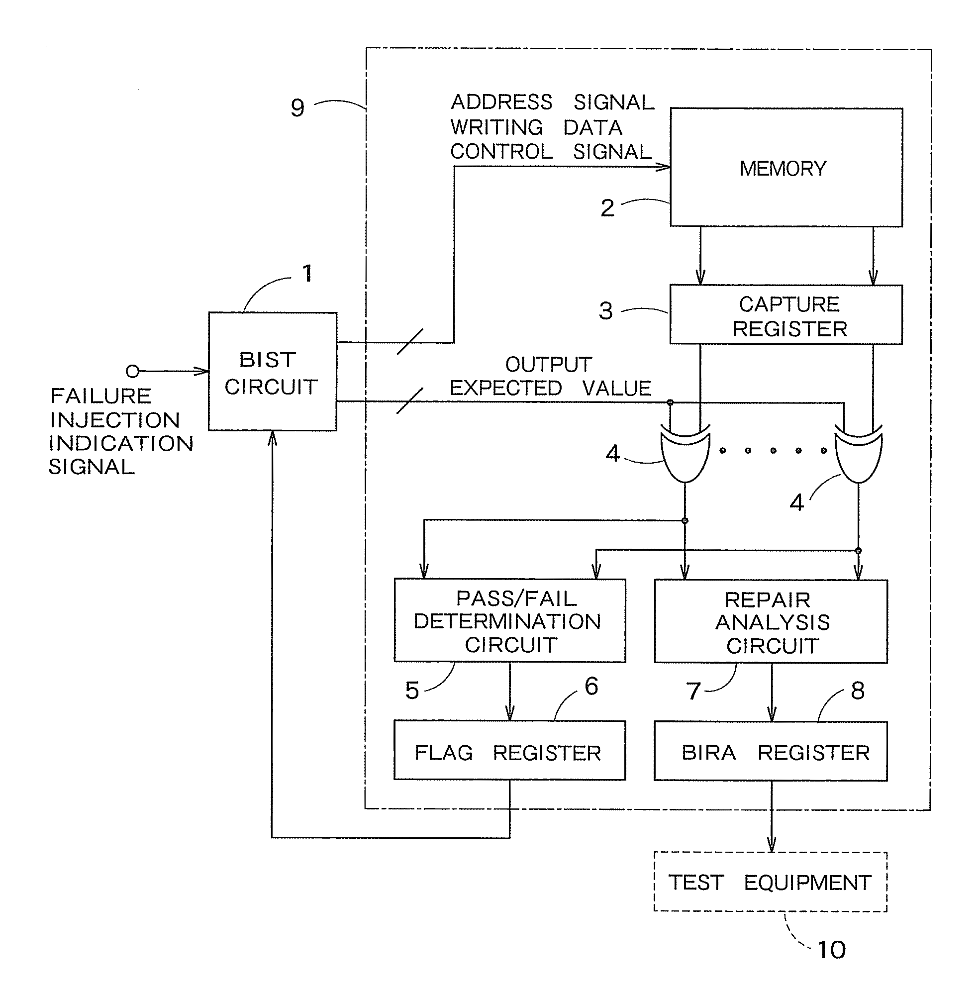
[0025]FIG. 1 is a block diagram showing a schematic configuration of a semiconductor integrated circuit according to a first embodiment of the present invention. The semiconductor integrated circuit of FIG. 1 has a BIST circuit 1, a memory 2, a capture register 3, comparison circuits 4, the number of which is the same as that of the bits of input / output data of the memory 2, a pass / fail determination circuit 5, a flag register 6, a repair analysis circuit 7, and a BIRA register 8. The components except the BIST circuit 1 are integrated in a memory collar 9.

[0026]The BIST circuit 1 and the memory collar 9 can be integrated in a chip or can be composed of different chips. The memory 2 is, for example, a DRAM (Dynamic Random Access Memory), an SRAM (Static Random Access Memory), or a Flash memory. However, the type of the memory is not especially limited.

[0027]The present embodiment proposes an example for performing function verifications of a pass / fail determination and a repair anal...

second embodiment

[0056]In the first embodiment, the failure bit(s) of one bit of fixed bits is injected in the first embodiment. On the other hand, in a second embodiment, which will be explained below, the BIST circuit 1c can inject the failure bits to an arbitrary bit position.

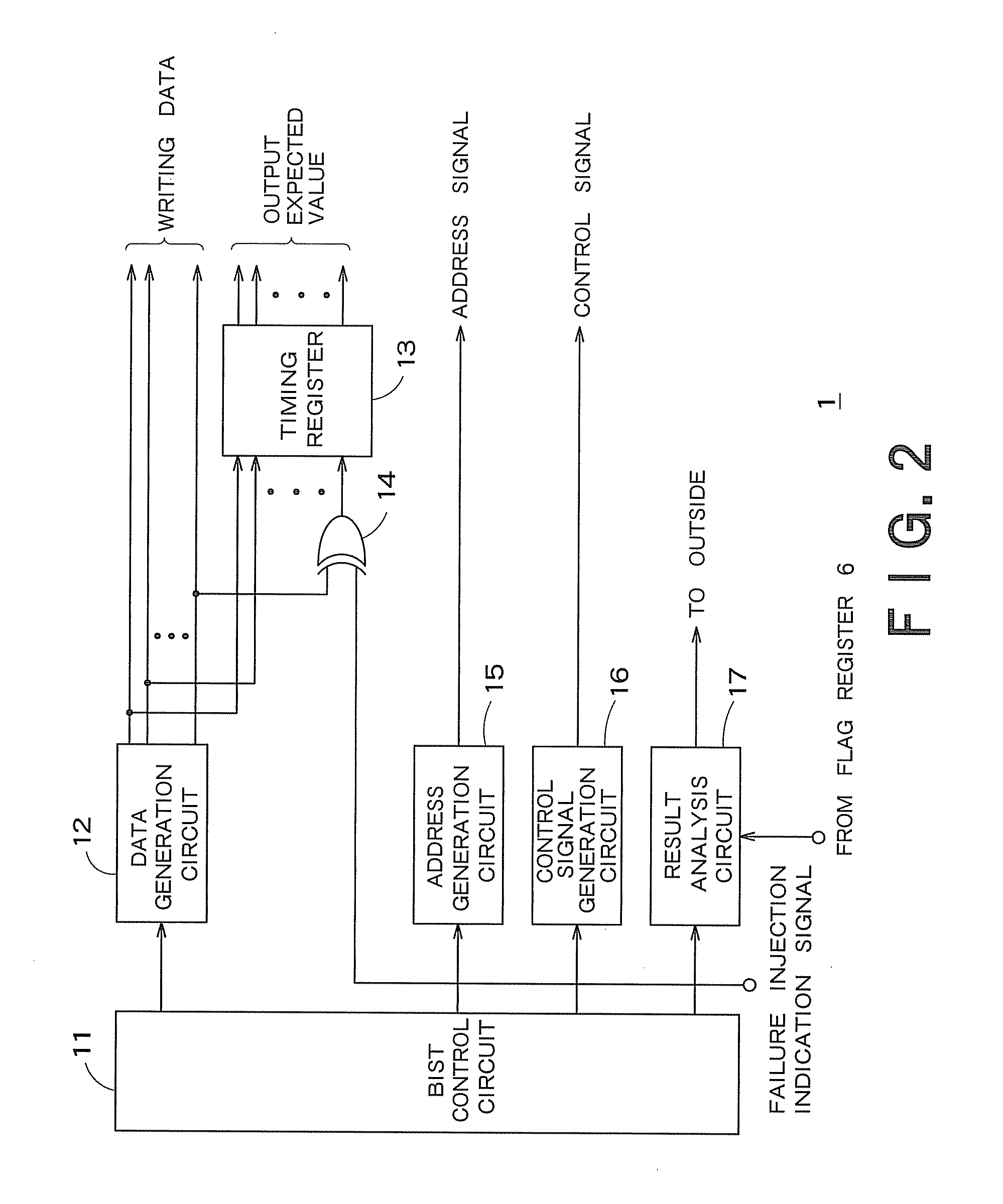
[0057]A schematic configuration of a semiconductor integrated circuit according to the second embodiment is the same as that of FIG. 1. However, an internal configuration of the BIST circuit 1c is different form that according the first embodiment. FIG. 5 is a block diagram showing an example of the internal configuration of the BIST circuit 1c according to the second embodiment of the present invention. In FIG. 5, components common to those of FIG. 2 have common reference numerals, respectively. Hereinafter, components different from FIG. 2 will be mainly described. The BIST circuit is of FIG. 5 has a failure data generation circuit 40 in addition to configurations of the BIST circuit 1 of FIG. 2.

[0058]The failure data gene...

third embodiment

[0081]The first and the second embodiments described above do not assume that the failure is set to a specific address in the memory 2, and the embodiments intends to set the bitline of the memory 2 to be in the failure state. On the other hand, a third embodiment, which will be explained hereinafter, sets a specific address in the memory 2 to be in the failure state.

[0082]FIG. 8 is a block diagram showing an example of an internal configuration of the BIST circuit 1d according to the third embodiment of the present invention. In FIG. 8, components common to those of FIG. 5 have common reference numerals, respectively. Hereinafter, components different from FIG. 5 will be mainly described.

[0083]The BIST circuit 1d of FIG. 8 is different from that of FIG. 5 in a technical feature that the address signal is inputted from the address generation circuit 15 to the failure bit setting circuit 21.

[0084]Furthermore, not only the failure injection indication signal, but a failure address set...


PUM


Abstract

A semiconductor integrated circuit has a data generation circuit configured to generate first data used for function verification of a built-in self test circuit and a built-in redundancy allocation circuit of a memory, a failure data generation circuit configured to generate second data for conducting a built in self test by inverting at least one bit of the first data based on a failure injection indication signal, and a timing circuit configured to adjust timing of at least one of the first and the second data in order to use one of the first and the second data as writing data to the memory and to use the other as an output expected value compared with data read out from the memory.

Description

CROSS REFERENCE TO RELATED APPLICATIONS[0001]This application is based upon and claims the benefit of priority from the prior Japanese Patent Applications No. 2009-71871 filed on Mar. 24, 2009, the entire contents of which are incorporated herein by reference.BACKGROUND OF THE INVENTION[0002]1. Field of the Invention[0003]The present invention relates to a semiconductor integrated circuit for conducting a self-test of a memory, a circuit function verification device and a method of verifying circuit function.[0004]2. Related Art[0005]In general, a pass / fail determination circuit and a repair analysis circuit are integrated in a semiconductor integrated circuit and a pass / fail determination and a redundancy analysis of a memory device are performed at the time of fabrication. A circuit for generating various types of signals for conducting the pass / fail determination and the redundancy analysis are called a built-in self test (hereinafter, referred to as MST) circuit and a built-in r...

Claims


Application Information

Patent Timeline
Patent Type & Authority Applications(United States)
IPC IPC(8): G11C29/04G06F11/22
CPCG11C29/02G11C29/028G11C29/12G11C29/1201G11C29/88G11C29/4401G11C29/50012G11C29/70G11C29/44
Inventor ANZOU, KENICHITOKUNAGA, CHIKAKO
Owner KK TOSHIBA
Why Eureka
Try Eureka