Data processing device, IC card and communication system

Inactive Publication Date: 2010-10-07
SEMICON ENERGY LAB CO LTD
View PDF50 Cites 10 Cited by
  • Summary
  • Abstract
  • Description
  • Claims
  • Application Information

AI Technical Summary

Benefits of technology

[0008]In the case of a data processing device having a contact-type terminal, since a large area of a conductive portion is exposed on a surface, a problem of an electrostatic breakdown of an internal circuit due to electrostatic discharge (ESD) (hereinafter, an electrostatic breakdown due to ESD is simply referred to as ESD in some cases) easily occurs.
[0009]In addition, in a non-contact data processing device which achieves multiple functions by providing of a CPU inside, dedicated design is required for a CPU portion of each function to be provided. Moreover, the more functions the non-contact data processing device has, the larger a circuit scale inside becomes; therefore, increase in power consumption easily becomes a problem. Specifically, among non-contact data processing devices that perform wireless communication without contact, a non-contact data processing device called a passive type which internally generates driving power from an alternating current signal used for transmission and reception consumes a large amount of power in an internal circuit, which greatly influences a communication distance.
[0010]In view of the above problems, it is an object to provide a data processing device which achieves multiple functions or easy additional providing of a function while suppressing adverse effect on a communication distance. Alternatively, it is another object to increase a resistance to electrostatic discharge in the data processing device.
[0020]According to the above-described means, a required function is provided by an external integrated circuit and the external integrated circuit is connected to a data processing device through a terminal portion thereof; therefore, the data processing device that achieves easy additional providing or easy replacement of a function can be provided. The terminal portion can have an adequate resistance to ESD by formation of a protection circuit inside the data processing device. Further, since integrated circuits with different functions can be formed and connected to the data processing device, an integrated circuit with a large scale does not need to be formed inside the data processing device in advance. Therefore, the data processing device can reduce power consumption and contribute to increase in a communication distance.

Problems solved by technology

In the case of a data processing device having a contact-type terminal, since a large area of a conductive portion is exposed on a surface, a problem of an electrostatic breakdown of an internal circuit due to electrostatic discharge (ESD) (hereinafter, an electrostatic breakdown due to ESD is simply referred to as ESD in some cases) easily occurs.
Moreover, the more functions the non-contact data processing device has, the larger a circuit scale inside becomes; therefore, increase in power consumption easily becomes a problem.
Specifically, among non-contact data processing devices that perform wireless communication without contact, a non-contact data processing device called a passive type which internally generates driving power from an alternating current signal used for transmission and reception consumes a large amount of power in an internal circuit, which greatly influences a communication distance.

Method used


Image

  • Data processing device, IC card and communication system
  • Data processing device, IC card and communication system
  • Data processing device, IC card and communication system

Examples


embodiment 1

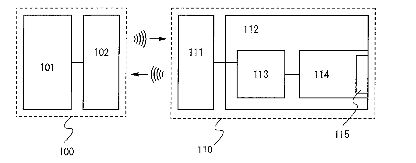
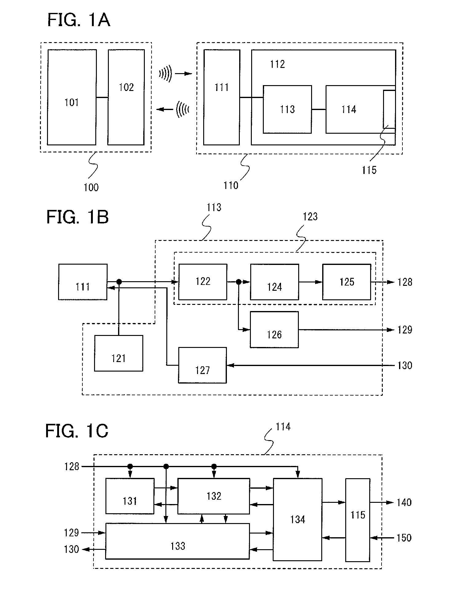
[0030]A structure of a data processing device in this embodiment is described.

[0031]FIG. 1A illustrates wireless communication between the data processing device and a reader / writer in this embodiment. A reader / writer 100 includes an antenna 102 for transmitting and receiving carrier waves or modulation waves through wireless communication, a functional circuit 101 for each processing in accordance with data extracted from the modulation waves, and the like. A data processing device 110 includes an antenna 111 and an integrated circuit 112 including functional circuits. The integrated circuit 112 includes an analog circuit 113 which performs generation of electric power, demodulation or modulation of a signal, or the like and a logic circuit 114 which mainly has a logic function. The logic circuit 114 includes a terminal portion 115 as described later.

[0032]Carrier waves are signals of alternating current waves which are also referred to as carriers. In wireless communication, the f...

embodiment 2

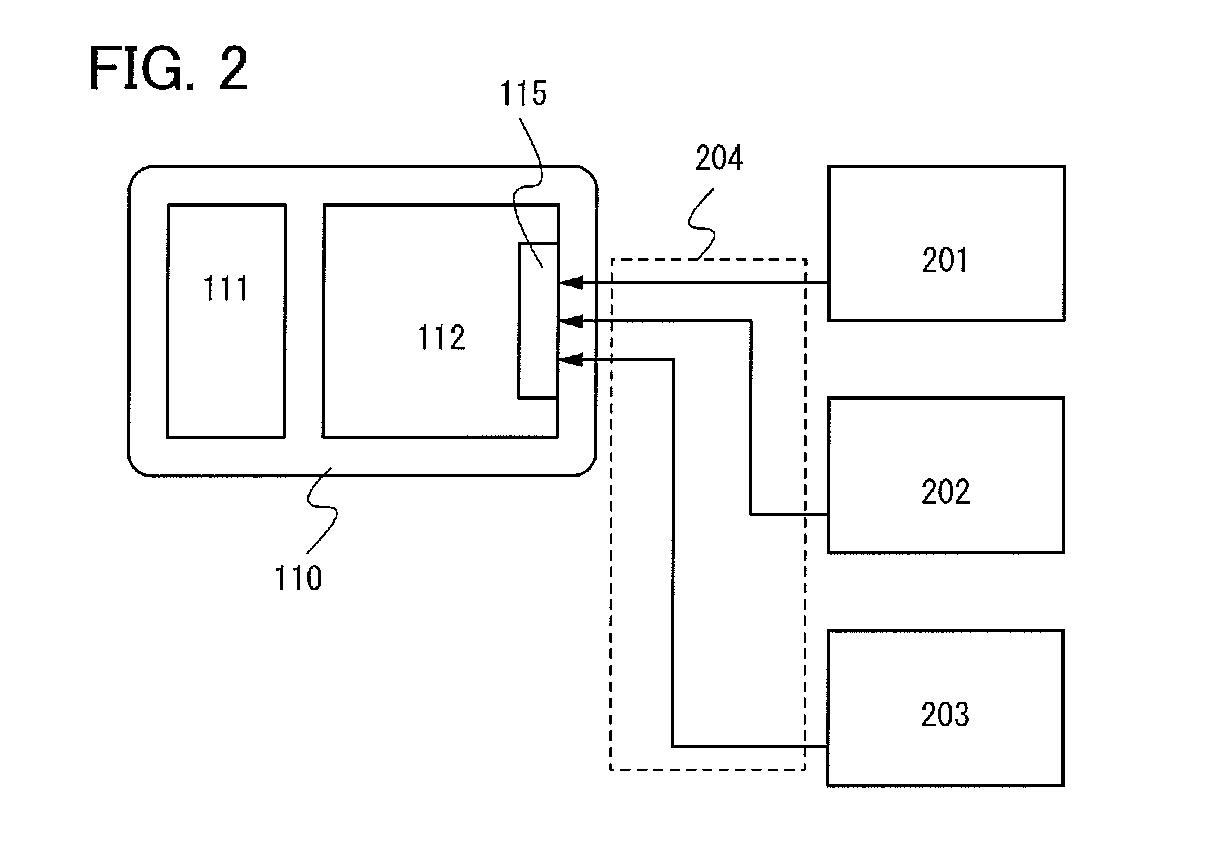
[0047]FIG. 2 illustrates a mode of connection between a data processing device in this embodiment and external devices. By connecting the data processing device 110 to an external device A201, an external device B202, or an external device C203 through the terminal portion 115 provided for the data processing device 110, a function of each of the external devices can be provided for the data processing device 110.

[0048]For example, in the case where the functions of the external devices A201 to C203 are different from each other and a usage environment differs in each of the functions, when a plurality of functions provided by the above described external device group is provided for the integrated circuit 112 in advance, a circuit scale naturally increases. Therefore, since the number of elements increases, increase in power consumption is inevitable. Although reduction in power consumption to some extent is possible by, for example, selectively supplying electric power to only som...

embodiment 3

[0054]A data processing device in FIG. 8 has a card shape by incorporating a data processing device including an antenna 803, an integrated circuit 802, and a terminal 804 in a base material 801 for supporting them. A data processing device having such a mode is referred to as an IC card or the like. The base material 801 is formed using a resin material or the like and integrated circuit 802 and the antenna 803 are embedded inside the base material 801 to be supported. In that case, the data processing device may have a supporting and fixing structure as shown by the reference numeral 805 for supporting and fixing external devices 810, 820, and 830 so as to avoid disconnection. In the case of FIG. 8, concave-shaped guides 805 are provided on the base material 801 (IC card) side and convex-shaped guides 813 are provided on the external device 810 side. The terminal 804 and the terminal 812 are connected to each other by sliding the external device into the base material 801 and enga...


PUM


Abstract

An object is to provide a data processing device which achieves multiple functions or easy additional providing of a function while suppressing adverse influence on a communication distance or to improve resistance to electrostatic discharge in the data processing device. The data processing device includes an antenna which transmits and receives a first signal to / from a first terminal device through wireless communication, an integrated circuit which executes a process in accordance with the first signal, and a terminal portion which transmits and receives a second signal to / from a second terminal device and has an exposed conductive portion on its surface. A protection circuit is provided between at least one terminal of terminals of the terminal portion and a power supply terminal of a high potential and between the one terminal and a power supply terminal of a low potential.

Description

BACKGROUND OF THE INVENTION[0001]1. Field of the Invention[0002]This specification relates to a data processing device for transmission and reception of data to / from a terminal device through wireless communication and communication system using the data processing device.[0003]2. Description of the Related Art[0004]In recent years, an environment where information network can be accessed at any time in any situations, which is referred to as a ubiquitous information society, has been facilitated. In such an environment, an individual identification technique has attracted attentions, such that an identification number (ID) is assigned to each object, whereby the history of the object is clarified and the production, management, or the like is facilitated. Above all, non-contact data processing devices capable of wirelessly transmitting and receiving data have started to be used.[0005]Individual object identification techniques which utilize an RFID (radio frequency identification) ...

Claims


Application Information

Patent Timeline
IPC IPC(8): H04Q5/22
CPCH04W52/028Y02D30/70
Inventor KOYAMA, JUNKATO, KIYOSHIYAMAZAKI, SHUNPEI
Owner SEMICON ENERGY LAB CO LTD
Why Eureka
Try Eureka