Semiconductor device and method of manufacturing the same

a technology of semiconductors and semiconductors, applied in the direction of semiconductor devices, electrical devices, transistors, etc., can solve the problems of increasing the impurity concentration required for obtaining the desired threshold voltage too much for a completely-depleted miniaturized fin, reducing mobility or increasing characteristic variation,

Inactive Publication Date: 2010-10-14
HITACHI LTD
View PDF5 Cites 20 Cited by
  • Summary
  • Abstract
  • Description
  • Claims
  • Application Information

AI Technical Summary

Benefits of technology

[0011]From the studies by the inventors as described above, it has been found out that, in the FINFET having an effective structure for suppressing the short-channel effect, a desired technique is to improve deterioration of transistor characteristics such as a variation of the threshold voltage as keeping the structure suitable for the miniaturization. Accordingly, a preferred aim of the present invention is to provide a technique of improving characteristics of a semiconductor device having a FINFET.
[0016]That is, characteristics of a semiconductor device having a FINFET can be improved.

Problems solved by technology

In a FINFET, it is difficult to design so-called multi Vth in which FETs having different threshold voltages from each other are arranged on the same substrate as performed in a bulk-MISFET.
A reason for the difficulty is that an impurity concentration required for obtaining a desired threshold voltage is increased too much for a completely-depleted miniaturized fin.
Also, a channel containing high-concentration impurity adversely causes decrease in mobility or increase in characteristic variation due to statistic fluctuation of the impurity.
In this manner, it has been found out that, current amount in the case is reduced by half compared with that of a conventional FINFET not using the back gate and using the both-side surfaces for the channel, and therefore, high-speed performance of a device is significantly damaged.
Also, it has been found out that the structure of providing two gates electrically isolated from each other on both-side surfaces of the miniaturized fin is not suitable for further miniaturization because of a viewpoint of securing a contact region or others.

Method used


Image

  • Semiconductor device and method of manufacturing the same
  • Semiconductor device and method of manufacturing the same
  • Semiconductor device and method of manufacturing the same

Examples


first embodiment

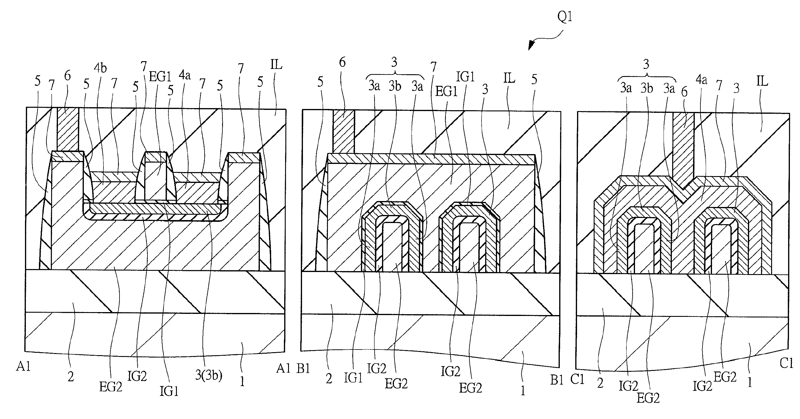
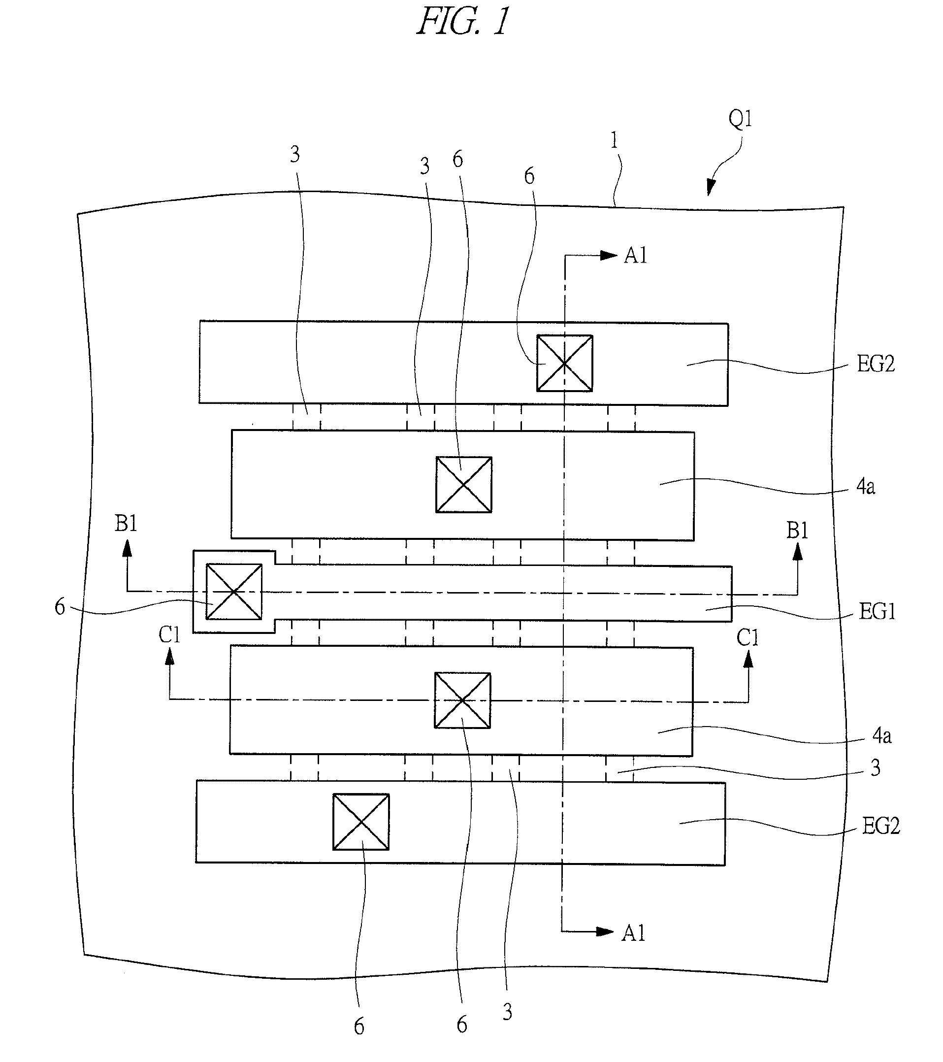
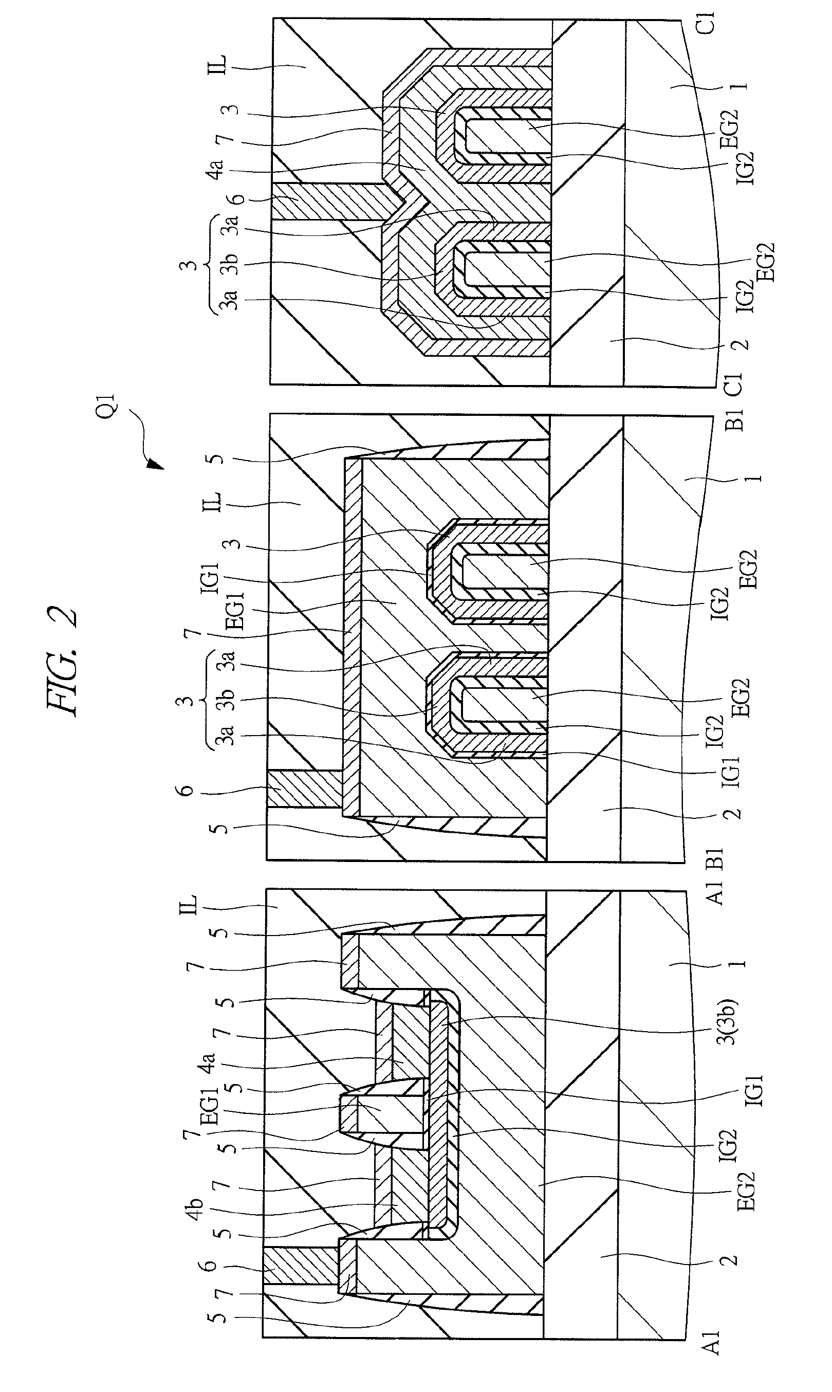
[0053]FIG. 1 illustrates a plan view of a principal part of a FINFET Q1 which a semiconductor device according to a first embodiment has. In FIG. 1, illustrations of a part of members such as an insulating film are omitted to easily see drawings. Also, FIG. 2 illustrates cross-sectional views of principal parts viewed in each arrow direction along lines A1-A1, B1-B1, and C1-C1 in the plan view of the principal part in FIG. 1. With reference to FIGS. 1 and 2, a structure of the FINFET Q1 according to the first embodiment will be described in detail. The FINFET Q1 which the semiconductor device according to the first embodiment has is formed on a silicon substrate (semiconductor substrate) 1, and has components described below.

[0054]On a main surface of the silicon substrate 1, an insulating layer 2 formed of an insulator mainly made of silicon oxide is formed. The FINFET Q1 according to the first embodiment is formed on the silicon substrate 1, more particularly, on the insulating la...

second embodiment

[0127]FIG. 24 illustrates cross-sectional views of principal parts of a FINFET Q3 which a semiconductor device according to a second embodiment has. The illustrated regions correspond to those in FIG. 2 in the FINFET Q1 according to the first embodiment, and their plan views of principal parts are the same as those in FIG. 1, and therefore, their plan views are not illustrated here. The FINFET Q3 illustrated in FIG. 24 is constitutionally the same as the FINFET Q1 described with reference to FIGS. 1 and 2 except for the following points, and effects obtained by having each component are also the same as the above-described effects.

[0128]The FINFET Q3 which the semiconductor device according to the second embodiment has is formed on a silicon substrate 1. And, a back-gate insulating film IG2 is formed between the silicon substrate 1 and a back gate electrode EG2, so that they are insulated from each other. As described in FIGS. 1 and 2, the back-gate insulating film IG2 is an insulat...

third embodiment

[0140]FIG. 30 illustrates cross-sectional views of principal parts of a FINFET Q4 which a semiconductor device according to a third embodiment has. The illustrated regions correspond to those in FIG. 2 in the FINFET Q1 according to the first embodiment, and their plan views of principal parts are the same as those in FIG. 1, and therefore, their plan views are not illustrated here. The FINFET Q4 illustrated in FIG. 30 is constitutionally the same as the FINFET Q1 described with reference to FIGS. 1 and 2 except for the following points, and effects obtained by having each component are also the same as the above-described effects.

[0141]A channel layer 3 of the FINFET Q4 which the semiconductor device according to the third embodiment has is arranged in a parallel-plane shape facing each other. This structure can be also described to have two channel sidewall portions 3a arranged in the direction crossing the main surface of the silicon substrate 1 and not to have the channel crosspi...


PUM


Abstract

Characteristics of a semiconductor device having a FINFET are improved. The FINFET has: a channel layer arranged in an arch shape on a semiconductor substrate and formed of monocrystalline silicon; a front gate electrode formed on a part of an outside of the channel layer through a front gate insulating film; and a back gate electrode formed so as to be buried inside the channel layer through a back gate insulating film. The back gate electrode arranged inside the arch shape is arranged so as to pass through the front gate electrode.

Description

CROSS-REFERENCE TO RELATED APPLICATION[0001]The present application claims priority from Japanese Patent Application No. JP 2009-098072 filed on Apr. 14, 2009, the content of which is hereby incorporated by reference into this application.TECHNICAL FIELD OF THE INVENTION[0002]The present invention relates to a semiconductor device and a method of manufacturing the same. More particularly, the present invention relates to a technique effectively applied to a semiconductor device having a FIN-type electric-field effect transistor (FET, simply called FINFET hereinafter) with a fin (FIN) shaped channel layer.BACKGROUND OF THE INVENTION[0003]As achieving a high-integrated and high-performed LSI, miniaturization for a metal insulator semiconductor (MIS) type FET (hereinafter, simply called MISFET) has been advanced. Due to scaling down of a gate length by the miniaturization, so-called short-channel effect problem has significantly arisen in which a threshold voltage Vth is lowered. The s...

Claims


Application Information

Patent Timeline
Patent Type & Authority Applications(United States)
IPC IPC(8): H01L29/78H01L21/336
CPCH01L29/785H01L29/66795
Inventor ISHIGAKI, TAKASHITSUCHIYA, RYUTAMORITA, YUSUKESUGII, NOBUYUKI
Owner HITACHI LTD
Why Eureka
Try Eureka