Method of manufacturing a semiconductor device

a semiconductor and manufacturing method technology, applied in semiconductor/solid-state device manufacturing, basic electric elements, electric devices, etc., can solve problems such as frequent physical contact between neighboring objects, contact failure, and insufficient contact between the interconnection and the conductive pattern

Inactive Publication Date: 2010-10-14
SAMSUNG ELECTRONICS CO LTD
View PDF19 Cites 9 Cited by
  • Summary
  • Abstract
  • Description
  • Claims
  • Application Information

AI Technical Summary

Benefits of technology

[0027]According to some example embodiments of the present general inventive concept, the second opening through which the interconnection may be exposed may be centrally self-aligned with the interconnection not by a photolithography process using a mask pattern but by etching rate difference between the first insulation interlayer and the second insulation interlayer, and thus the upper conductive pattern may be centrally self-aligned with the interconnection automatically. Thus, various process defects caused by mis-alignment between the interconnection and the upper conductive pattern may be sufficiently prevented.

Problems solved by technology

That is, a slight mis-alignment between the interconnection and the conductive pattern would mostly lead to contact failure or insufficient contact between the interconnection and the conductive pattern.
Further, the slight mis-alignment between the interconnection and the conductive pattern would also lead to a frequent physical contact between neighboring interconnections, which is widely known as a bridge defect, since the line interval between the neighboring interconnections are largely decreased.
Particularly, a central alignment between an interconnection and an upper conductive structure has been strongly needed in a wiring process for a semiconductor device in view of the current manufacturing environments in which a slight and minute mis-alignment between the interconnection and the upper conductive structure results in the bridge defect.

Method used


Image

  • Method of manufacturing a semiconductor device
  • Method of manufacturing a semiconductor device
  • Method of manufacturing a semiconductor device

Examples


Embodiment Construction

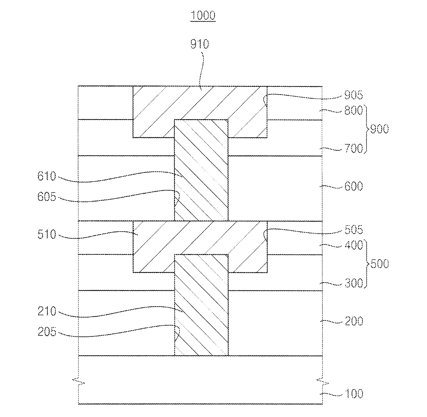
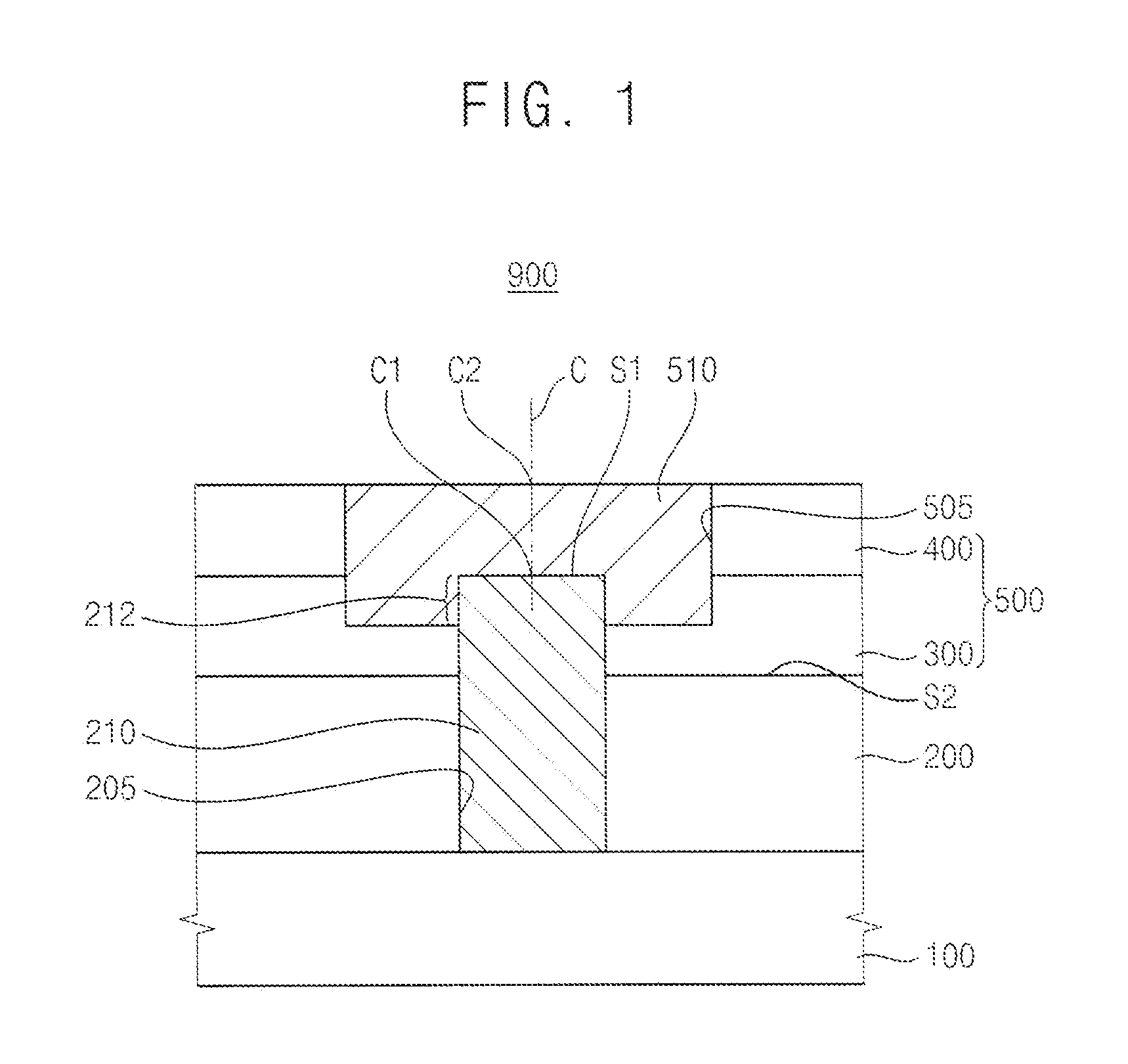
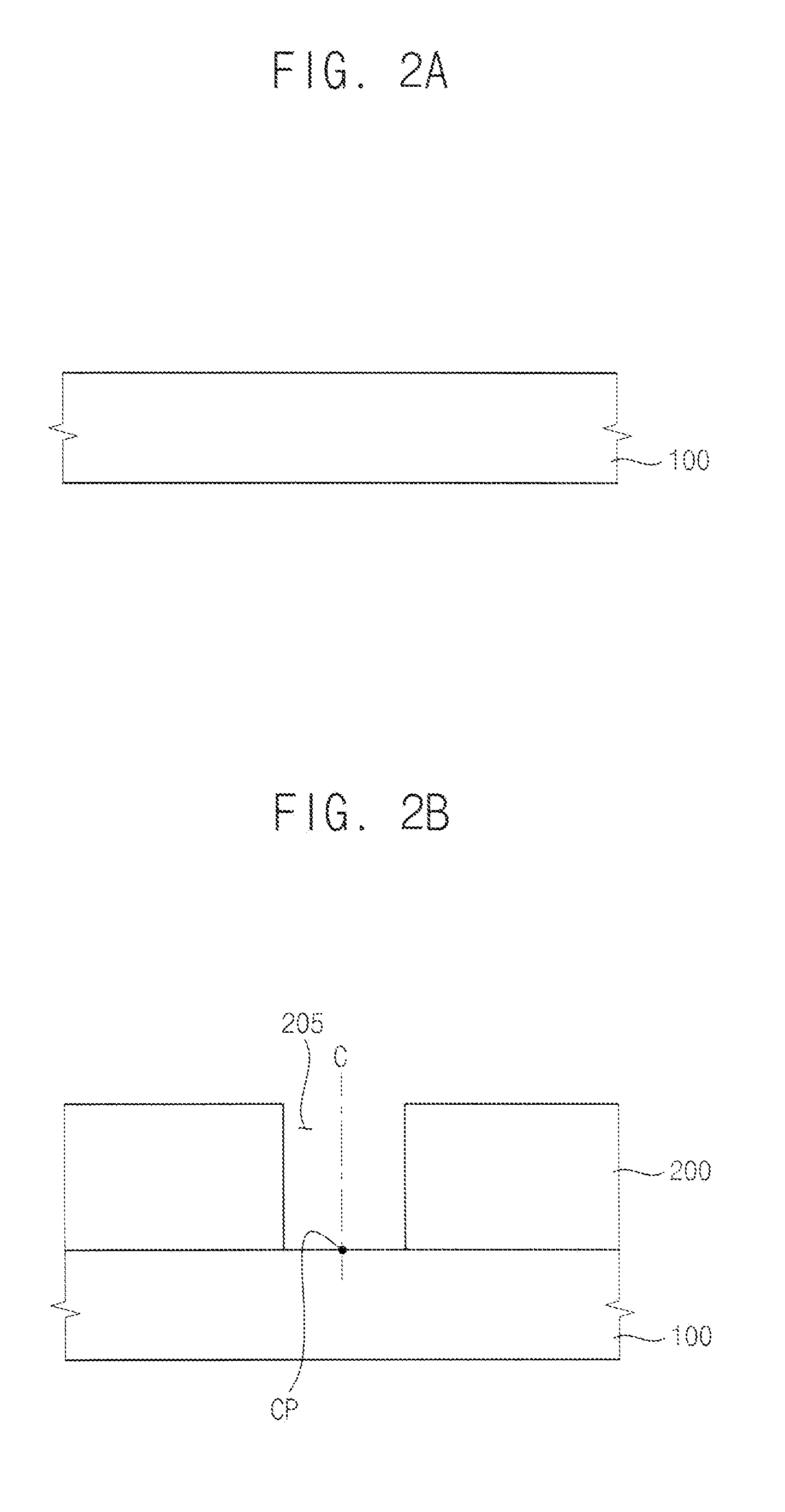
[0032]Various example embodiments will be described more fully hereinafter with reference to the accompanying drawings, in which some example embodiments are illustrated. The present general inventive concept may, however, be embodied in many different forms and should not be construed as limited to the example embodiments set forth herein. Rather, these example embodiments are provided so that this disclosure will be thorough and complete, and will fully convey the scope of the present general inventive concept to those skilled in the art. In the drawings, the sizes and relative sizes of layers and regions may be exaggerated for clarity.

[0033]Reference will now be made in detail to the embodiments of the present general inventive concept, examples of which are illustrated in the accompanying drawings, wherein like reference numerals refer to the like elements throughout. The embodiments are described below in order to explain the present general inventive concept by referring to th...


PUM


Abstract

In a semiconductor device and method of manufacturing thereof, a first insulation interlayer is formed on a substrate including a lower conductive pattern. The first insulation interlayer has a first opening through which the lower conductive pattern is exposed. An interconnection is formed in the first opening such that the interconnection is contact with the lower conductive pattern and protruded from the first insulation interlayer. A second insulation interlayer is formed on the first insulation interlayer in such a manner that the second insulation interlayer has a second opening through the interconnection is exposed and the second opening is centrally aligned with the interconnection. An upper conductive pattern is formed in the second opening such that the upper conductive pattern is contacted with the interconnection. Accordingly, a mis-alignment between the upper conductive pattern and the interconnection is prevented.

Description

CROSS-REFERENCE TO RELATED APPLICATIONS[0001]This application claims priority under 35 U.S.C. §119 from Korean Patent Application No. 2009-31065, filed on Apr. 10, 2009 in the Korean Intellectual Property Office (KIPO), the contents of which are herein incorporated by reference in their entirety.BACKGROUND[0002]1. Field of the General Inventive Concept[0003]Example embodiments relate to a semiconductor device and a method of manufacturing the same, and more particularly, to a semiconductor device having a wiring interconnections and methods of manufacturing the same.[0004]2. Description of the Related Art[0005]Recently, unit devices of an integrated circuit, such as conductive structures of a memory device, are vertically and sequentially stacked on a substrate in a medium of an insulation interlayer and lower and upper unit devices are electrically connected to each other through a conductive interconnection such as a contact plug or a via plug in accordance with device requirement...

Claims


Application Information

Patent Timeline
Patent Type & Authority Applications(United States)
IPC IPC(8): H01L21/768
CPCH01L21/76897H01L21/76885H01L21/3205H01L21/28H01L21/768
Inventor NA, JONG-JIN
Owner SAMSUNG ELECTRONICS CO LTD
Why Eureka
Try Eureka