Adhesive film and method for encapsulating organic electronic device using same

a technology of adhesive film and organic electronic device, which is applied in the direction of heat-activated film/foil adhesive, film/foil adhesive without carrier, application, etc., can solve the problems of poor adhesion and release properties, product including an oled may be very sensitive to environmental conditions, and the durability of oleds is not good, so as to prevent the effect of process defects

Active Publication Date: 2015-05-28
LG CHEM LTD
View PDF8 Cites 6 Cited by
  • Summary
  • Abstract
  • Description
  • Claims
  • Application Information

AI Technical Summary

Benefits of technology

[0012]When an organic electronic device is encapsulated using an adhesive film according to the exemplary embodiments of the present invention, failures, such as lifting or chipping, occurring in a process of peeling a protection film and / or a release film can be suppressed, and process defects can be prevented.

Problems solved by technology

The most significant problem in commercialization and pervasive use of OLEDs is durability.
Accordingly, a product including an OLED may be very sensitive to environmental conditions.
However, since an existing adhesive film for encapsulating an OLED is formed in a single layer disposed between two release films, adhesion and release properties are very poor.
In particular, as the size of the adhesive film increases due to a growth in size of an OLED, a failure rate in peeling of the adhesive film during a process of encapsulating the OLED increases.
For example, a peeling failure, such as lifting of the adhesive film, may occur when a protection film or a release film is peeled.
Although release films having different peeling properties have been used, it is not enough to solve the problem.

Method used


Image

  • Adhesive film and method for encapsulating organic electronic device using same
  • Adhesive film and method for encapsulating organic electronic device using same
  • Adhesive film and method for encapsulating organic electronic device using same

Examples


example 1

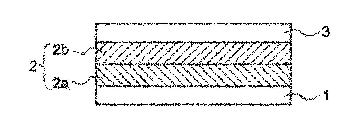
[0084]1. Preparation of First Adhesive Layer Solution

[0085]As a moisture adsorbent solution, CaO (Sigma-Aldrich Co. LLC.) was added into methyl ethyl ketone at a concentration of 30 wt % to prepare a moisture adsorbent solution, and then the solution was milled for 24 hours in a ball mill process.

[0086]60 parts by weight of BPA-type liquid YD-128 (Kukdo Chemical Co. Ltd.) as an epoxy resin, 0.1 parts by weight of KBM-403 (Shin-Etsu Chemical Co. Ltd.) as a surface additive, and 40 parts by weight of YP-70 (Kukdo Chemical Co., Ltd.) as a high molecular weight resin having a softening point of 40° C. or more were added to prepare a homogenized solution. 6 parts by weight of 2PZ-CNS (Shikoku Chemicals Corp.) was added as a curing agent to the homogenized solution.

[0087]5 parts by weight with respect to the resin of the milling solution was added to the homogenized solution, and methyl ethyl ketone was added until the total solid content was about 50%, followed by high-speed stirring for...

example 2

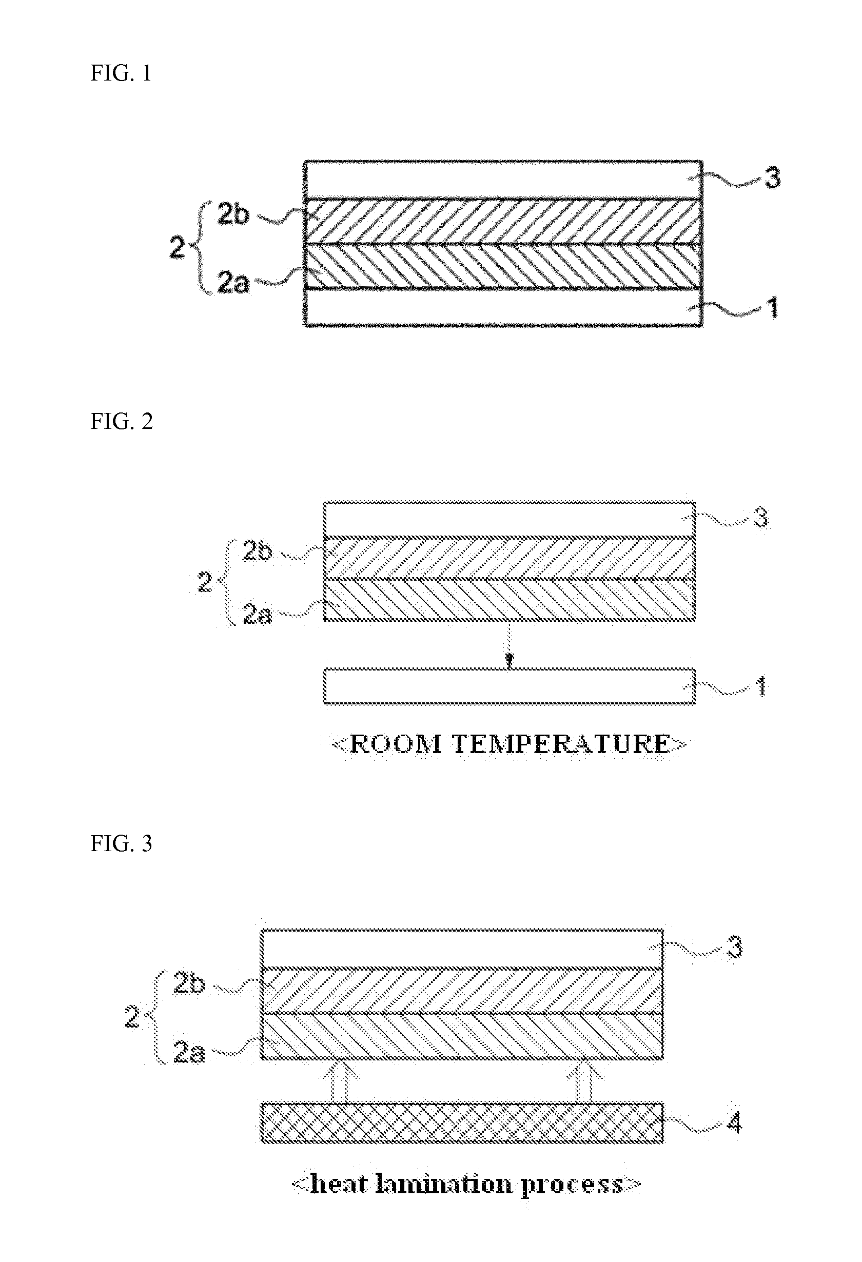
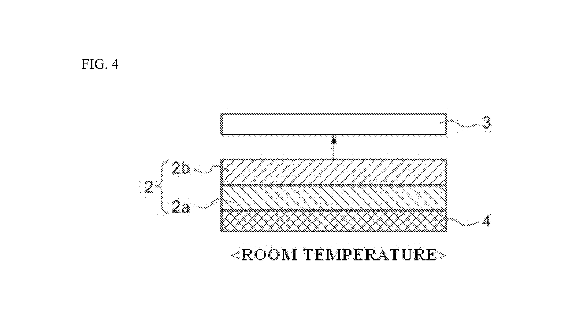
[0096]A multilayered adhesive film was prepared using the same method as described in Example 1, except that the weight ratios of the surface additives in the first adhesive layer and the second adhesive layer are different from those in the process of preparing the adhesive film of Example 1. That is, in Example 2, the content of the surface additive in the first adhesive layer increased to 0.2 parts by weight, and the content of the surface additive in the second adhesive layer increased to 0.5 parts by weight.

example 3

[0097]A multilayered adhesive film was prepared using the same method as described in Example 1, except that the weight ratios of the epoxy resin in the first adhesive layer and the second adhesive layer are different from those in the process of preparing the adhesive film of Example 1. That is, in Example 3, the content ratio of a liquid epoxy and a high molecular weight resin in the first adhesive layer was changed to 65:35, and the content ratio of the liquid epoxy and the high molecular weight resin in the second adhesive layer was changed to 62:38.


PUM

PropertyMeasurementUnit
adhesiveaaaaaaaaaa
peeling strengthaaaaaaaaaa
molecular weightaaaaaaaaaa

Abstract

The present invention relates to an adhesive film, to an encapsulated product of an organic electronic device using same and to a method for encapsulating an organic electronic device using same. More particularly, an adhesive film for encapsulating an organic electronic device comprises: a protective film layer, a first adhesive layer, a second adhesive layer and a release film layer sequentially arranged. The peel strength (A) between the first adhesive layer and the protective film layer is lower than the peel strength (B) between the second adhesive layer and the release film layer, and the peel strength (B) between the second adhesive layer and the release film layer is lower than the peel strength (C) between the first adhesive layer and an encapsulation substrate, thus improving faults during a peeling process.

Description

TECHNICAL FIELD[0001]The present invention relates to an adhesive film and a method of encapsulating an organic electronic device using the same.BACKGROUND ART[0002]An organic electronic device (OED) refers to an device including an organic material layer generating a charge flow using holes and electrons, for example, a photovoltaic device, a rectifier, a transmitter, or an organic light emitting diode (OLED).[0003]Among the organic electronic devices, OLEDs have less power consumption and a higher response speed than other light sources, and has advantages in fabricating a thin display device or illuminating device. In addition, since OLEDs have excellent space utilization, OLEDs are expected to be applied to various fields, such as various portable devices, monitors, laptops, and TVs.[0004]The most significant problem in commercialization and pervasive use of OLEDs is durability. Organic materials and metal electrodes included in an OLED may be very easily oxidized by an external...

Claims


Application Information

Patent Timeline
Patent Type & Authority Applications(United States)
IPC IPC(8): H01L51/52C09J163/00C09J7/02B32B38/10B32B37/18C09J7/10
CPCH01L51/5253B32B38/10B32B37/18C09J2463/00C09J7/0207C09J163/00C09J7/02C09J2203/326B32B37/025B32B37/12B32B2310/0806B32B2457/206C09J7/10Y10T428/1471C09J2301/208C09J2301/302C09J2301/312H10K50/844C09J7/35C09J7/22C09J7/40C09J201/00C09J133/00C09J167/00C09J11/08
Inventor BAE, KYUNG YULYOO, HYUN JEELEE, SEUNG MINCHO, YOON GYUNGCHANG, SUK KYSHIM, JUNG SUP
Owner LG CHEM LTD
Why Eureka
Try Eureka