Method for accessing storage apparatus and related control circuit

a storage apparatus and control circuit technology, applied in the field of bad block management, can solve the problems of unsatisfactory read/write speed, flash memory cell breakage, and whole block not working normally, and achieve the effect of low efficiency

Inactive Publication Date: 2010-10-14
JMICRON
View PDF4 Cites 311 Cited by
  • Summary
  • Abstract
  • Description
  • Claims
  • Application Information

AI Technical Summary

Benefits of technology

[0009]With this in mind, it is one objective of the present invention to overcome the conventional bad block management method problem of low efficiency for a multi-channel SSD. The present invention provides an innovative bad block management method and a related control circuit to overcome the problems encountered by the conventional method.
[0010]According to one exemplary embodiment of the present invention, a method for accessing a storage apparatus is provided. The storage apparatus has a plurality of storage units respectively corresponding to a plurality of access channels, wherein each storage unit respectively has a plurality of blocks and the plurality of access channels operate simultaneously in a data access operation. In addition, the plurality of storage units includes a first storage unit and at least one second storage unit. The method comprises: generating a plurality of bad block lists respectively corresponding to the plurality of storage units according to bad blocks that cannot operate normally in the plurality of storage units; according to at least one bad block indicated by a bad block list of the first storage unit, configuring a good block that corresponds to the bad block and can operate normally in each second storage unit as a replacement block; generating a corresponding mapping result according to a bad block list and each replacement block of each second storage unit; and accessing the storage apparatus according to the bad block list of the first storage unit and the mapping result of each second storage unit.
[0011]According to another exemplary embodiment of the present invention, a control circuit for accessing a storage apparatus is provided. The storage apparatus has a plurality of storage units respectively corresponding to a plurality of access channels, wherein each storage unit respectively has a plurality of blocks, and the plurality of access channels operate simultaneously in a data access operation. In addition, the plurality of storage units includes a first storage unit and at least one second storage unit. The control circuit comprises: a processing unit, a storing unit and a plurality of mapping units. The processing unit is for generating a plurality of bad block lists respectively corresponding to the plurality of storage units according to bad blocks that cannot operate normally in the plurality of storage units. Furthermore, according to at least one bad block indicated by a bad block list of the first storage unit, the processing unit configures a good block that corresponds to the bad block and can operate normally in each second storage unit as a replacement block and generates a corresponding mapping result according to a bad block list and each replacement block of each second storage unit. The storing unit is coupled to the processing unit and is utilized for storing the bad block lists. The plurality of mapping units are respectively coupled to the processing unit and the plurality of storage units and are respectively configured by the plurality of corresponding mapping results, wherein the control circuit accesses the plurality of storage units through the plurality of mapping units and the bad block list of the first storage unit.

Problems solved by technology

Compared with maturely-developed traditional hard disks, however, flash memories still have many shortcomings that need to be overcome, one of which is an unsatisfactory read / write speed.
However, during the fabrication or the actual operation of the flash memory, the flash memory cell may be broken.
Since an erase operation upon the flash memory must be performed by blocks, a broken flash memory cell will mean the whole block cannot work normally.
If one block in a certain flash memory is skipped, the skip block method will skip all the corresponding blocks in other flash memories, which wastes the storage space of the multi-channel SSD.
Thus, the skip block method is not very economical for the multi-channel SSD.
However, this method causes an overhead of the control circuit.
Moreover, the control circuit needs to replace the bad block with the replacement block one by one according to remapping results, which could cause severe latency.
However, this method inevitably increases the fabrication costs of the flash memory since these additional reserved blocks cannot be utilized for data storage.

Method used


Image

  • Method for accessing storage apparatus and related control circuit
  • Method for accessing storage apparatus and related control circuit
  • Method for accessing storage apparatus and related control circuit

Examples


Embodiment Construction

[0017]Certain terms are used throughout the following description and claims to refer to particular system components. As one skilled in the art will appreciate, manufacturers may refer to a component by different names. This document does not intend to distinguish between components that differ in name but not differ in functionality. In the following discussion and in the claims, the terms “include”, “including”, “comprise”, and “comprising” are used in an open-ended fashion, and thus should be interpreted to mean “including, but not limited to . . . ” The terms “couple” and “coupled” are intended to mean either an indirect or a direct electrical connection. Thus, if a first device couples to a second device, that connection may be through a direct electrical connection, or through an indirect electrical connection via other devices and connections.

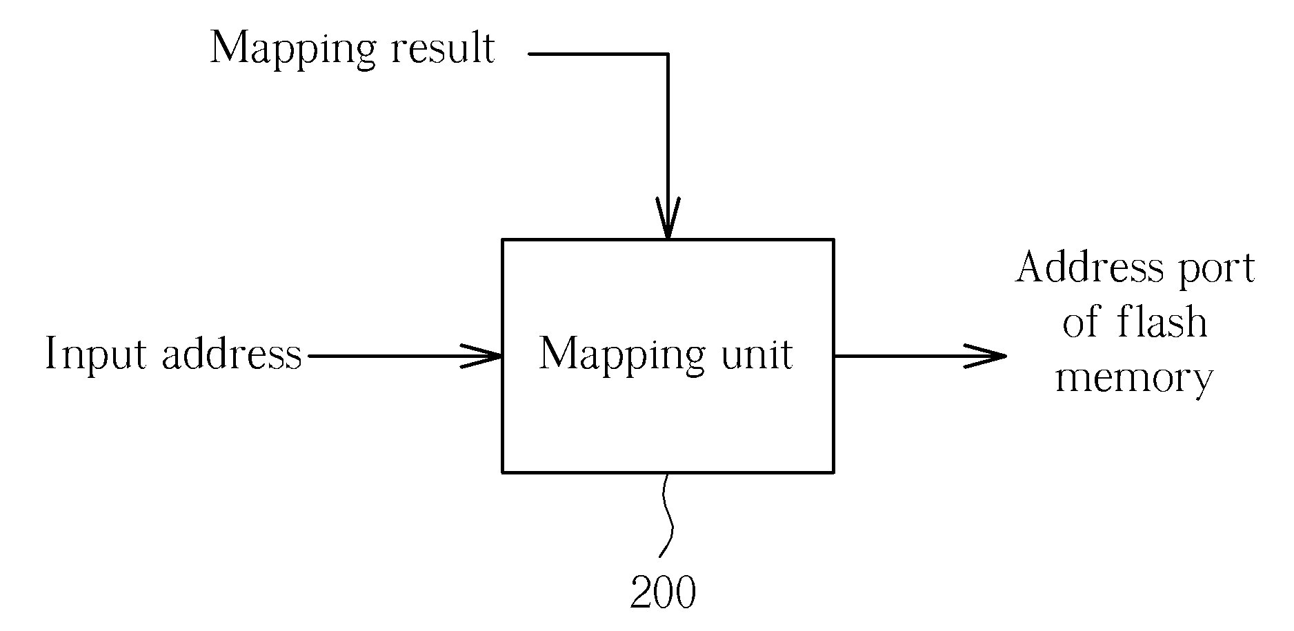
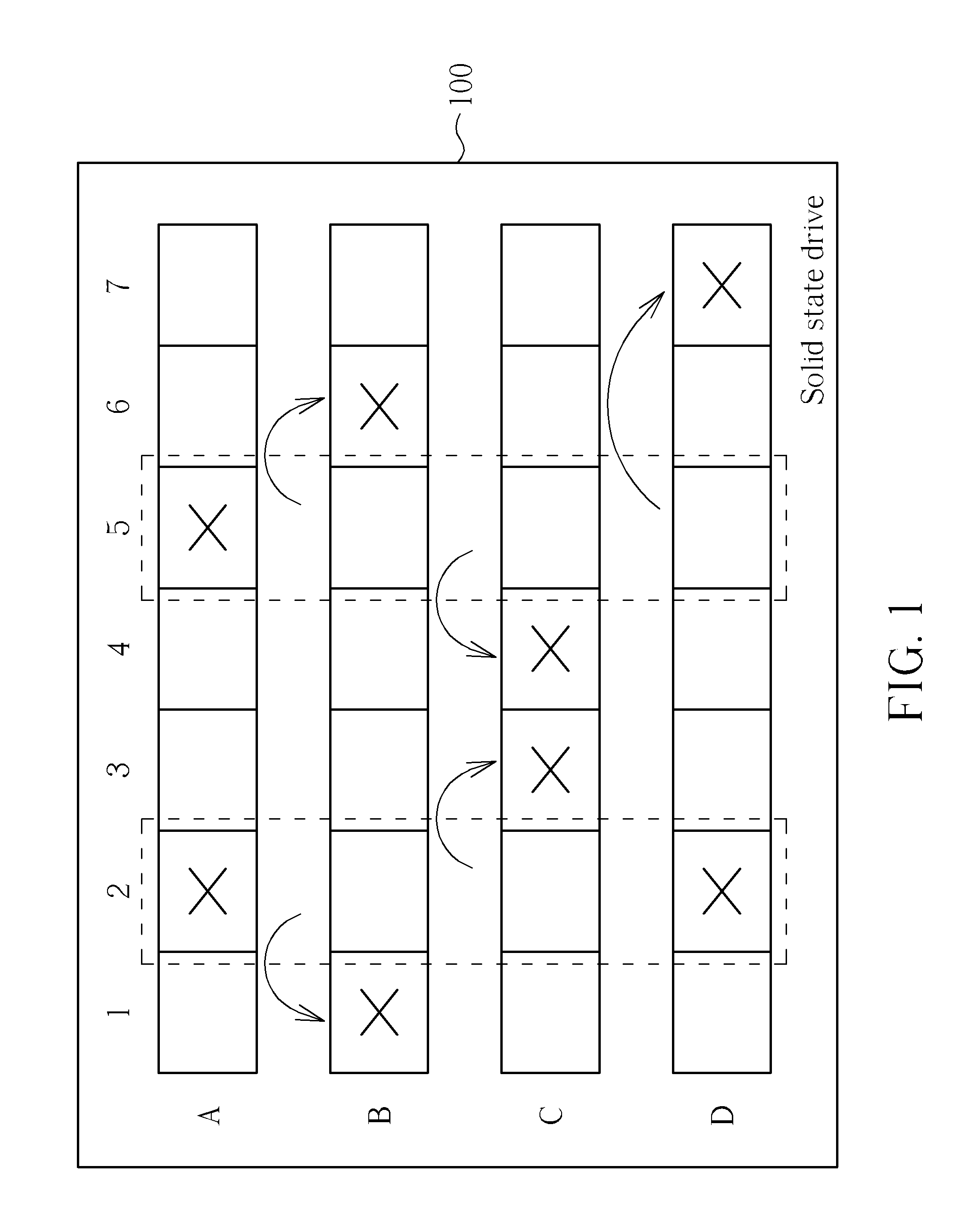
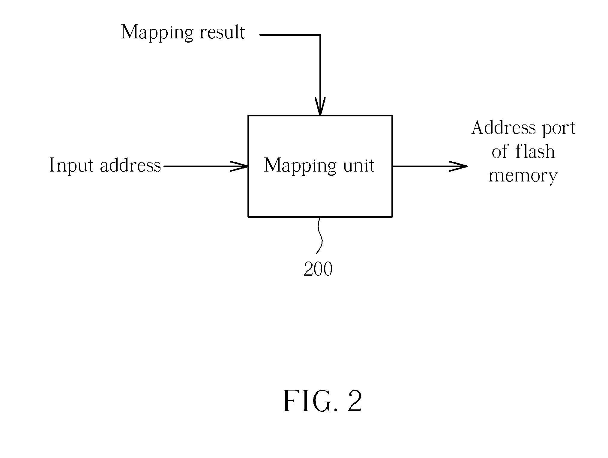
[0018]Please refer to FIG. 1, which is a diagram illustrating an exemplary embodiment of the method of the present invention. As shown...


PUM


Abstract

A storage apparatus includes a first storage unit and at least a second storage unit. A method for accessing the storage apparatus generates a plurality of bad block lists regarding the plurality of the storage units, respectively, and according to at least one bad block indicated by a bad block list of the first storage unit, configures at least a good block in each second storage unit corresponding to the at least one bad block of the first storage unit as a replacement block of each second storage unit. Accordingly, the method generates a mapping result of each second storage unit according to a bad block list of the second storage unit and each replacement block, and accesses the storage apparatus according to the bad block list of the first storage unit and each mapping result.

Description

BACKGROUND OF THE INVENTION[0001]1. Field of the Invention[0002]The present invention relates to bad block management, and more particularly, to a method and a related circuit utilized in a storage apparatus having a plurality of flash memories (e.g. a multi-channel solid state drive) for the purpose of bad block management.[0003]2. Description of the Prior Art[0004]Storage apparatus composed of flash memories are widely used in embedded systems and portable electronic devices. As storage apparatus of larger capacity and higher efficiency has become a requirement, the flash memory apparatus has been developed. In recent times, flash memory apparatus have started to replace conventional storage apparatus (e.g. hard disks). One such flash memory apparatus is the solid state drive (SSD), which is a mass storage apparatus composed of flash memories, and is positioned to replace the traditional hard disk.[0005]Compared with maturely-developed traditional hard disks, however, flash memori...

Claims


Application Information

Patent Timeline
Patent Type & Authority Applications(United States)
IPC IPC(8): G06F12/00
CPCG06F12/0246G06F2212/7205G06F2212/7202G06F2212/7201
Inventor LIU, CHAO-YINWANG, SHENG-HSUAN
Owner JMICRON
Why Eureka
Try Eureka