Information input device and display device

a technology of information input and display device, which is applied in the direction of instruments, transmission systems, computing, etc., can solve the problems of lowering the detection sensitivity, the difficulty of high accuracy in detecting the touch position, and the need to increase the width of the detecting electrode, so as to facilitate detection and achieve high accuracy

Active Publication Date: 2010-10-21
JAPAN DISPLAY INC
View PDF29 Cites 170 Cited by
  • Summary
  • Abstract
  • Description
  • Claims
  • Application Information

AI Technical Summary

Benefits of technology

[0024]The embodiments of the present invention can provide a display device and an information input device that can easily realize detection with high accuracy.

Problems solved by technology

However, in the case of the above-described capacitive touch sensor, its detection sensitivity is often not sufficiently high and thus it is often difficult to detect the touch position with high accuracy.
For example, if the electrostatic capacitance based on the scanning electrode and the detecting electrode is significantly lower than the parasitic capacitance of the detector, the detection is often not favorable, which causes the need to increase the width of the detecting electrode.
However, in this case, the fringe electric field is blocked by this wide detecting electrode, and thus the lowering of the detection sensitivity often Occurs.
This often results in a long detection time.
As above, the touch sensor often involves insufficient detection sensitivity and a long detection time, and therefore it is often difficult for the touch sensor to perform the detection with high accuracy.

Method used


Image

  • Information input device and display device
  • Information input device and display device
  • Information input device and display device

Examples


first embodiment

1. First Embodiment

2. Second Embodiment

3. Third Embodiment

4. Fourth Embodiment

5. Fifth Embodiment

6. Others

1. First Embodiment

(A) Configuration of Display Device

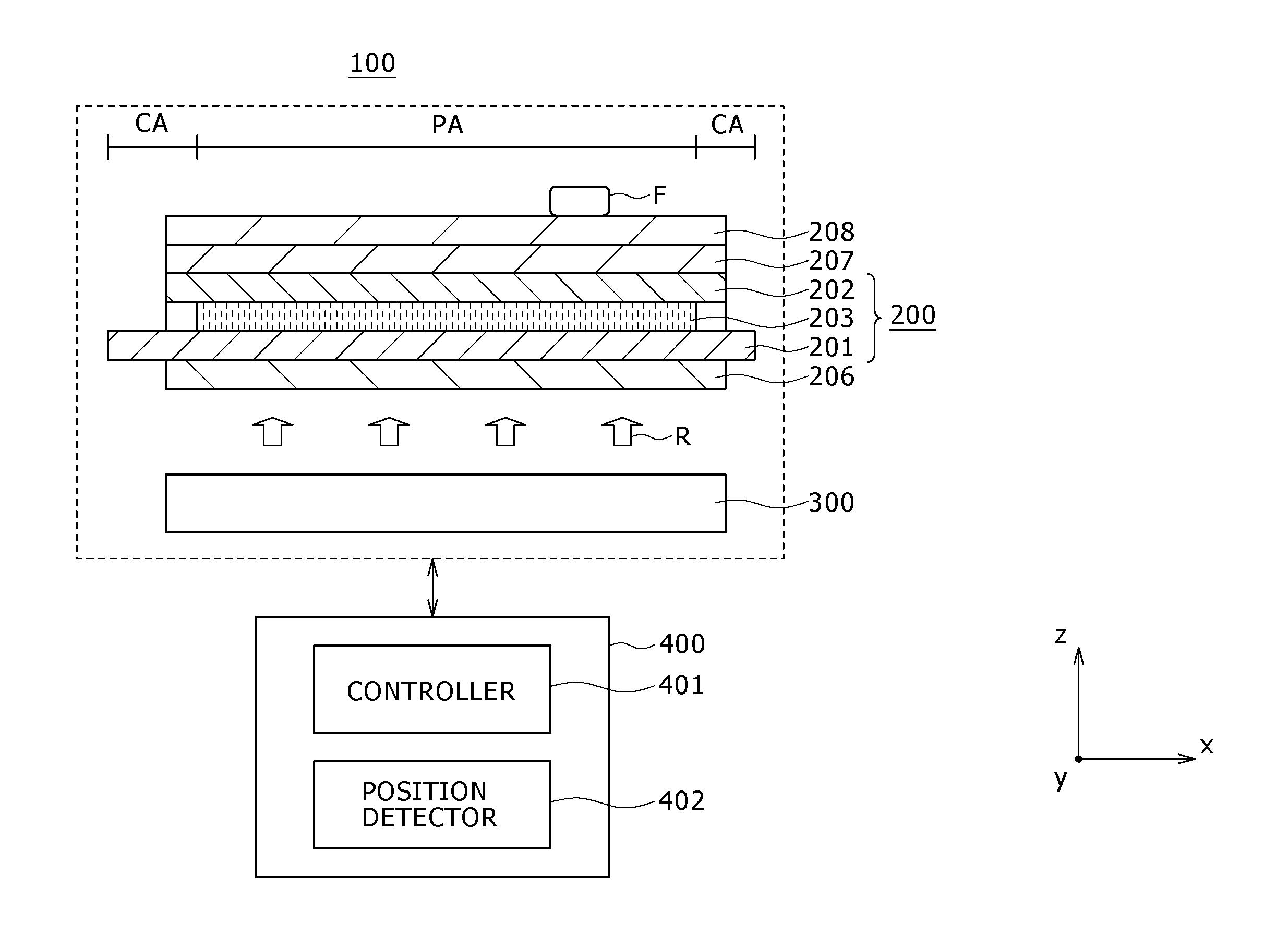
[0057]FIG. 1 is a diagram showing the outline of the configuration of a display device 100 in a first embodiment of the present invention.

[0058]As shown in FIG. 1, the display device 100 of the present embodiment has a liquid crystal panel 200, a backlight 300, and a data processor 400. These respective units will be sequentially described below.

(A-1) Liquid Crystal Panel

[0059]The liquid crystal panel 200 is based on e.g. the active-matrix system and has a TFT array substrate 201, a counter substrate 202, and a liquid crystal layer 203 as shown in FIG. 1. In the liquid crystal panel 200, the TFT array substrate 201 and the counter substrate 202 are opposed to each other at an interval therebetween. The liquid crystal layer 203 is provided between these substrates.

[0060]For the liquid crystal panel 200, as shown in FIG. 1, a f...

second embodiment

2. Second Embodiment

[0189]A second embodiment of the present invention will be described below.

(A) Detailed Configuration of Liquid Crystal Panel

[0190]The detailed configuration of a liquid crystal panel 200b in the present embodiment will be described.

[0191]FIG. 14 and FIG. 15 are diagrams showing major parts of the liquid crystal panel 200b in the second embodiment of the present invention.

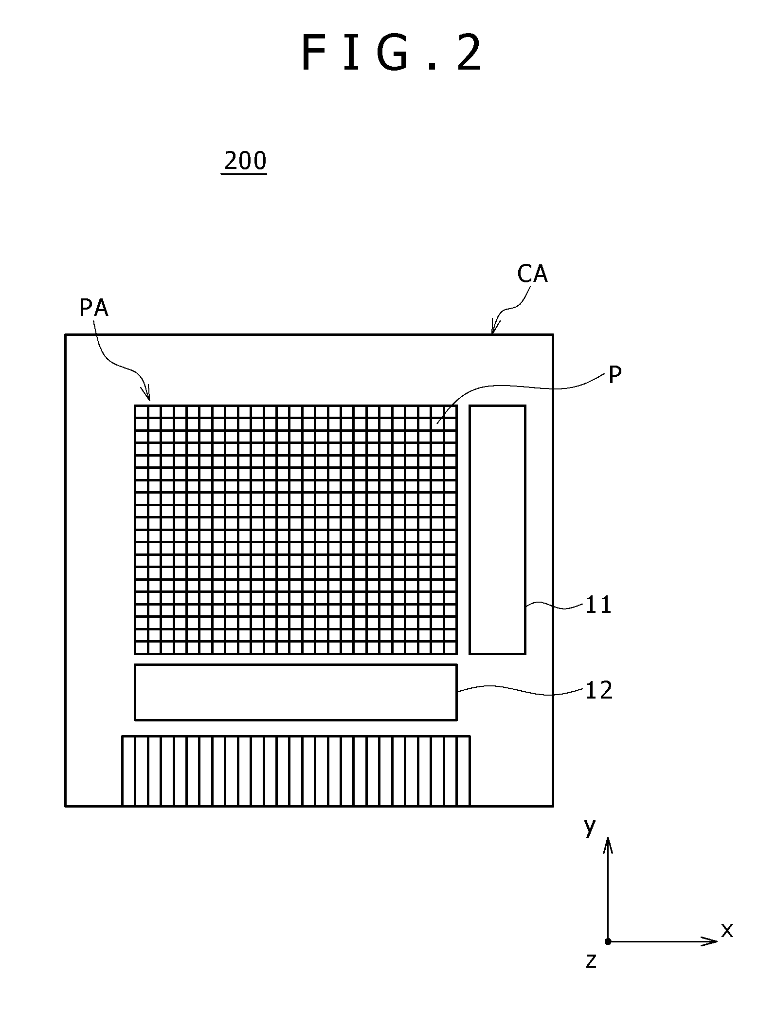
[0192]FIG. 14 is a sectional view schematically showing the outline of pixels P provided in a display area PA in the liquid crystal panel 200b according to the second embodiment of the present invention.

[0193]FIG. 15 is a top view schematically showing the outline of the pixel P provided in the display area PA in the liquid crystal panel 200b according to the second embodiment of the present invention.

[0194]As shown in FIG. 14 and FIG. 15, in the liquid crystal panel 200b of the present embodiment, pixel electrodes 62pb and counter electrodes 23b are so formed as to conform to the fringe field s...

third embodiment

3. Third Embodiment

[0212]A third embodiment of the present invention will be described below.

[0213]FIG. 17 is a diagram showing the outline of the configuration of a display device 100c in the third embodiment of the present invention.

[0214]As shown in FIG. 17, in the display device 100c of the present embodiment, a liquid crystal panel 200c is different from the liquid crystal panel 200 in the first embodiment. Furthermore, a touch panel 209 is further disposed over the liquid crystal panel 200c. Except for these points and points relating thereto, the third embodiment is the same as the first embodiment. Therefore, description of the overlapping part is omitted.

(A) Configuration of Liquid Crystal Panel

[0215]The configuration of the liquid crystal panel 200c will be described.

[0216]FIG. 18 is a diagram showing the configuration of the liquid crystal panel 200c in the third embodiment of the present invention. FIG. 18 is a sectional view schematically showing the outline of pixels P...


PUM


Abstract

An information input device includes a touch panel configured to be provided with a touch sensor that detects a position at which a sensing object is brought close to a sensing surface. In this information input device, the touch sensor has a scanning electrode and a detecting electrode that is opposed to the scanning electrode with the intermediary of a dielectric substance, and is a capacitive sensor whose electrostatic capacitance changes if the sensing object is brought close to the detecting electrode. Furthermore, a slit is formed in a surface of the detecting electrode opposed to the scanning electrode.

Description

BACKGROUND OF THE INVENTION[0001]1. Field of the Invention[0002]The present invention relates to information input devices and display devices, and particularly to an information input device and a display device including a panel provided with a capacitive touch sensor for detecting the position to which an object to be sensed is brought close.[0003]2. Description of the Related Art[0004]Display devices such as liquid crystal display devices and organic EL display devices have advantages such as small thickness, light weight, and low power consumption. Therefore, these display devices are frequently used in mobile-use electronic apparatus such as cellular phones and digital cameras.[0005]As one kind of such display devices, the liquid crystal display device has a liquid crystal panel formed by enclosing a liquid crystal layer between a pair of substrates as a display panel. The liquid crystal panel is e.g. a transmissive panel. Specifically, illuminating light emitted from an illum...

Claims


Application Information

Patent Timeline
Patent Type & Authority Applications(United States)
IPC IPC(8): G06F3/045
CPCG06F3/044G02F1/13338G06F3/04166G06F3/0446G02F1/133528G02F1/134309G02F1/13439G02F1/1368G02F2201/121G02F2201/123G02F2203/01G06F3/0412G06F3/0416G06F2203/04101G06F2203/04103G06F2203/04108G06F2203/04111G09G5/18G09G2300/0426
Inventor NAKANISHI, TAKAYUKINOGUCHI, KOJIISHIZAKI, KOJITERANISHI, YASUYUKITAKEUCHI, TAKEYA
Owner JAPAN DISPLAY INC
Why Eureka
Try Eureka