
Carbon nanotubes for the selective transfer of heat from electronics

a technology of carbon nanotubes and electronics, applied in the field of nanotube fabrics, can solve the problems of increasing the need for smaller and more potent heat transfer devices, high localized heating of integrated circuits, and the use of individual nanotubes for heat transfer

Active Publication Date: 2010-10-21
NANTERO
View PDF57 Cites 21 Cited by
  • Summary
  • Abstract
  • Description
  • Claims
  • Application Information

AI Technical Summary

Benefits of technology

The present invention provides carbon nanotubes for the selective transfer of heat from electronics. The nanotubes are in thermal contact with a circuit element and a thermal reservoir, allowing the nanotubes to transfer heat from the circuit element to the reservoir. The nanotube article has a non-woven fabric of nanotubes in contact with each other, with a density and shape selected to transfer heat at a pre-defined rate. The nanotube article can be deposited on the circuit element using pre-formed nanotubes or grown nanotubes on the surface of the circuit element. The invention also includes a method of forming a thermal management structure for an integrated circuit by depositing a layer of pre-formed nanotubes on the integrated circuit. The nanotubes have a nanotube density and shape selected to transfer heat at a pre-defined rate. The invention provides a solution for managing heat in integrated circuits, improving their performance and reliability.

Problems solved by technology

As ultra-large-scale-integration of integrated circuits, microelectronic components and devices are becoming increasingly more dense and compact, there exists an increasing need for smaller and more potent heat transfer devices due to the excessive on-chip heat generation.
Such power densities lead to highly localized heating of integrated circuits in areas known as “hot spots”.
Using individual nanotubes for heat transfer, however, can be problematic because of difficulties in growing them with suitably controlled orientation, length, and the like.

Method used


Image

  • Carbon nanotubes for the selective transfer of heat from electronics
  • Carbon nanotubes for the selective transfer of heat from electronics
  • Carbon nanotubes for the selective transfer of heat from electronics

Examples


Embodiment Construction

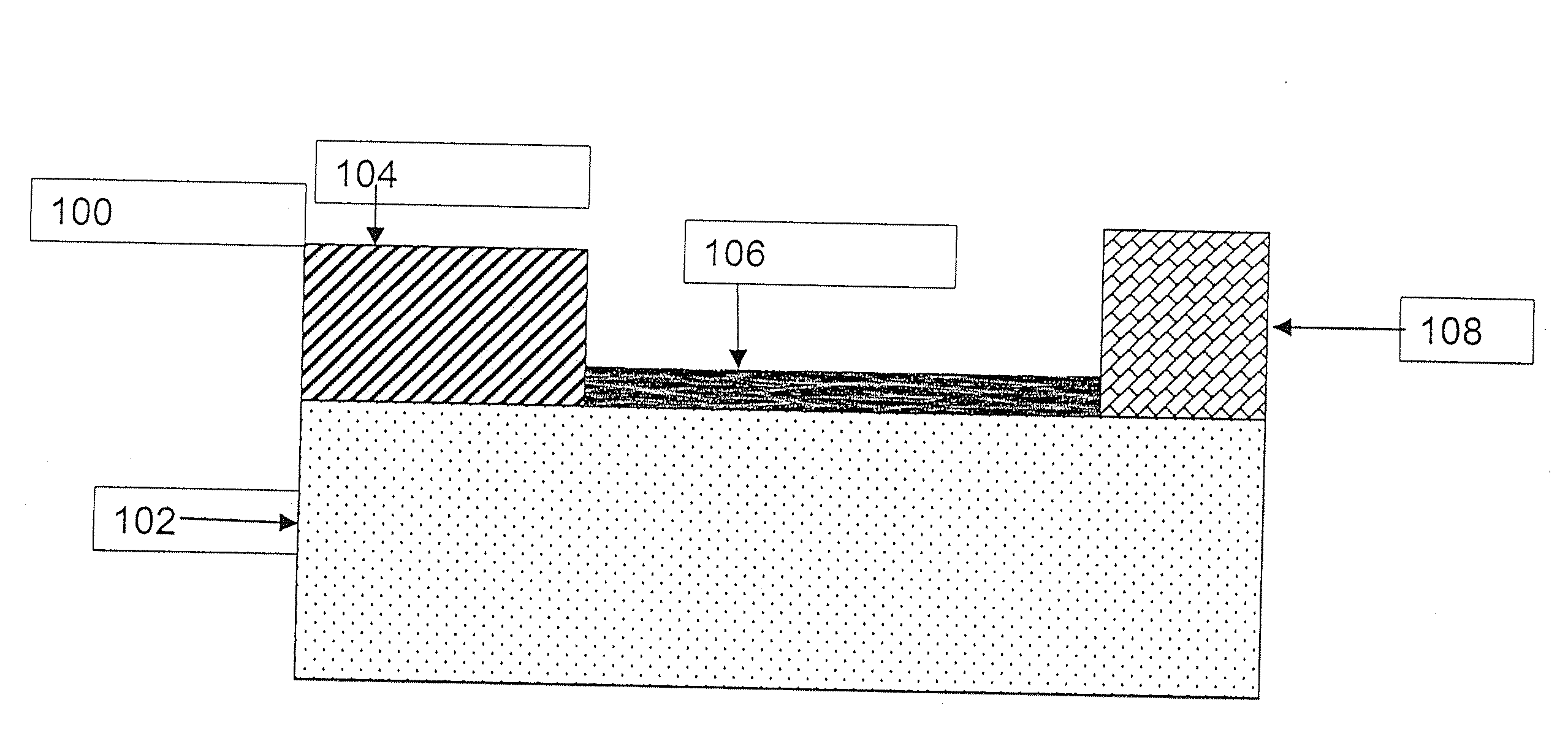
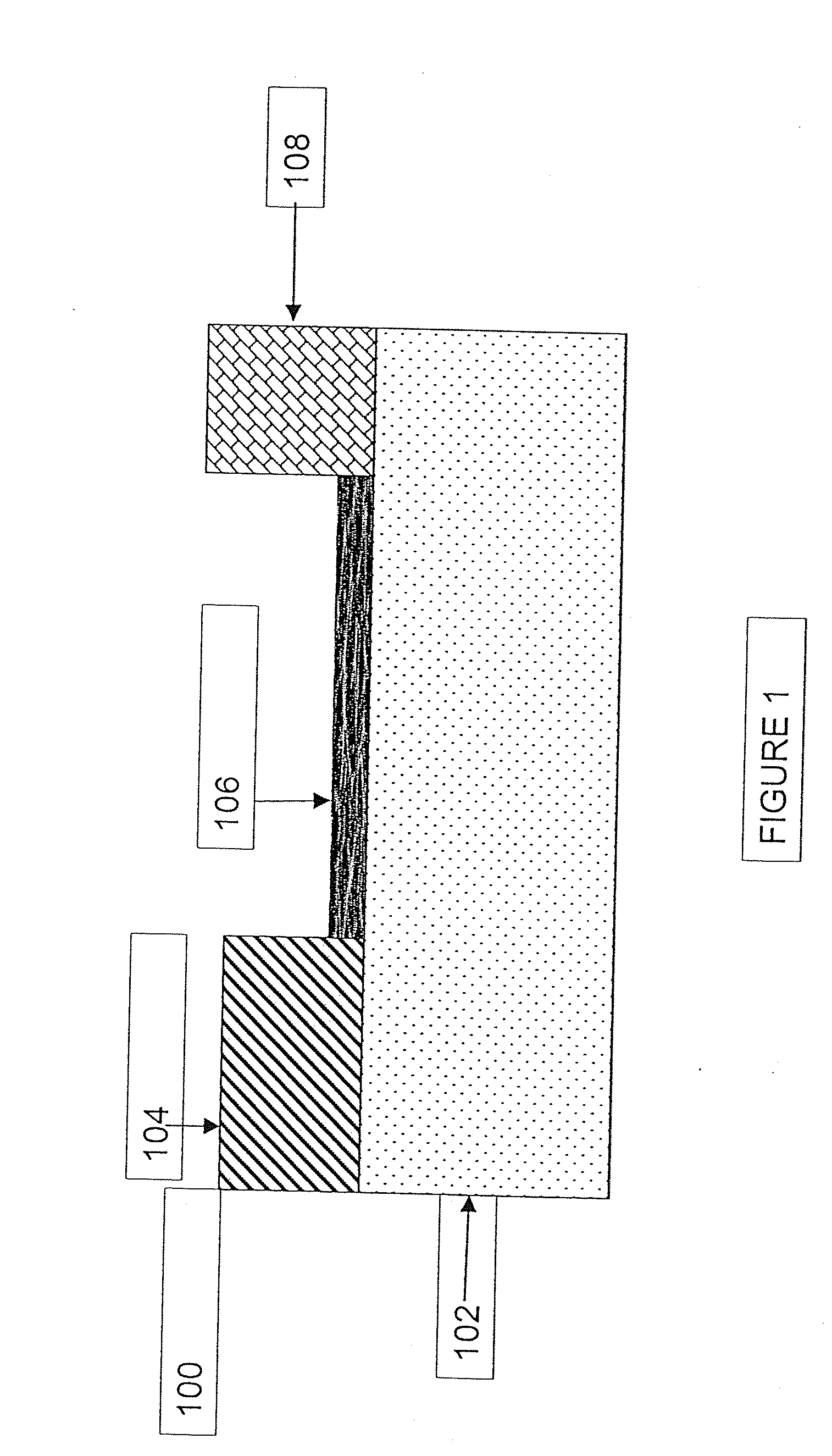
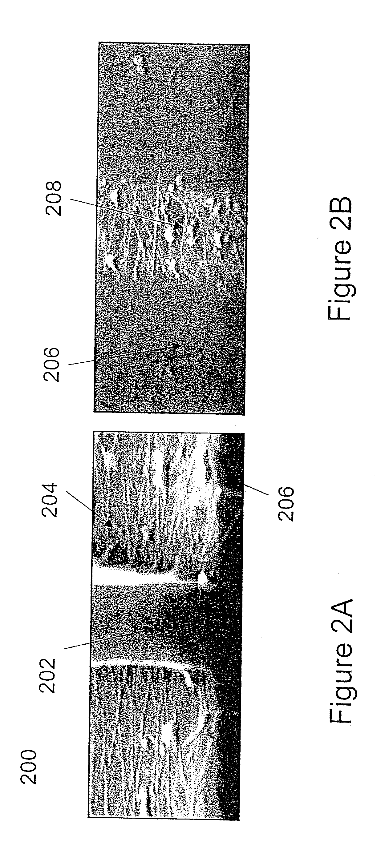
[0026]Non-woven fabrics of carbon nanotubes (CNTs) can help manage the problem of thermal “hot spots” and heat transfer in high power devices. CNT fabrics have superior thermal conductance relative to single nanotube as well as to conventional conductive materials such as metals, and therefore the CNT fabrics have a tremendous potential for providing extremely efficient heat transfer. CNTs exhibit a very high “axial” thermal conductivity. For a discrete multiwalled nanotube (MWNT), the thermal conductivity is expected to surpass 3000 W / m-k along the tube axis, while theoretical studies of single walled nanotubes (SWNTs) have shown that thermal conductivities of 6600 W / m-K are possible. CNT fabrics can be used as effective heat-sinks, which are able to remove large amounts of heat away from critical “hot spots”.

[0027]Preferred embodiments of this invention use CNT fabrics for the transfer of heat away from heat sensitive areas in an electronic circuit or from an entire electronic chi...


PUM

PropertyMeasurementUnit
lengthaaaaaaaaaa
thicknessaaaaaaaaaa
thicknessaaaaaaaaaa

Abstract

Under one aspect, a method of cooling a circuit element includes providing a thermal reservoir having a temperature lower than an operating temperature of the circuit element; and providing a nanotube article in thermal contact with the circuit element and with the reservoir, the nanotube article including a non-woven fabric of nanotubes in contact with other nanotubes to define a plurality of thermal pathways along the article, the nanotube article having a nanotube density and a shape selected such that the nanotube article is capable of transferring heat from the circuit element to the thermal reservoir.

Description

CROSS-REFERENCE TO RELATED APPLICATIONS[0001]This application claims the benefit under 35 U.S.C. §119(e) of U.S. Provisional Patent Application No. 60 / 714,386, filed Sep. 6, 2005 and entitled “Carbon Nanotubes for the Selective Transfer of Heat from Electronics,” the entire contents of which are incorporated herein by reference.BACKGROUND[0002]1. Technical Field[0003]The present application relates generally to nanotube fabrics and methods of making same.[0004]2. Discussion of Related Art[0005]As ultra-large-scale-integration of integrated circuits, microelectronic components and devices are becoming increasingly more dense and compact, there exists an increasing need for smaller and more potent heat transfer devices due to the excessive on-chip heat generation. Current integrated circuits used in microprocessors operated at high frequencies use power densities on the order of 50 W / cm2: in comparison, a 60 W light bulb generates 0.5 W / cm2. Such power densities lead to highly localiz...

Claims


Application Information

Patent Timeline
Patent Type & Authority Applications(United States)
IPC IPC(8): H01L23/373H01L21/70H01L21/02H10K99/00
CPCH01L23/373H01L23/433H01L2924/1306H01L24/28H01L24/31H01L2224/16H01L2224/73253H01L2924/01005H01L2924/01013H01L2924/01015H01L2924/01029H01L2924/01074H01L2924/01079H01L2924/01082H01L2924/14H01L2924/01006H01L2924/01019H01L2924/01023H01L2924/01033Y10S977/80H01L2924/00H01L2224/05573H01L2224/05568H01L2924/00014H01L2224/0554H01L2224/05599H01L2224/0555H01L2224/0556
Inventor WARD, JONATHAN W.BERTIN, CLAUDE L.SEGAL, BRENT M.
Owner NANTERO
Learn More