Da converter, solid-state imaging device, and camera system

a solid-state imaging and converter technology, applied in the field of da converters, solid-state imaging devices, and camera systems, can solve problems such as noise sources, achieve the effects of reducing the influence of current output, thermal noise or 1/f noise generated, and increasing circuit dimensions

Active Publication Date: 2010-10-28
SONY CORP
View PDF8 Cites 13 Cited by
  • Summary
  • Abstract
  • Description
  • Claims
  • Application Information

AI Technical Summary

Benefits of technology

[0022]Therefore, the current-controlled DA converter described above needs to include components such as LPFs or BPFs (Band-Pass Filters) for suppressing the influence of noise appearing in the reference voltage Vref; specifically, large capacitors or resistor elements are necessary.
[0024]Moreover, the use of the output signal Vout of the current-controlled DA converter as the reference voltage (RAMP) of the AD converter of the solid-state imaging device may cause the following disadvantages.
[0026]It is therefore desirable to provide a DA converter capable of reducing the influence on a current output, of thermal noise or 1 / f noise generated in a device without increasing a circuit dimension and thus achieving improvement in image quality. It is also desirable to provide a solid-state imaging device and a camera system employing the DA converter.
[0030]According to the embodiments of the present invention, it is possible to reduce the influence on a current output, of thermal noise or 1 / f noise generated in a device without increasing a circuit dimension and to thus achieve improvement in image quality.

Problems solved by technology

However, in the above-described DA converter, thermal noise or 1 / f noise generated in the circuit is superimposed in the reference voltage Vref being used, which may propagate through the basic current source cell to become a source of noise appearing in the output signal.
Moreover, the reference current generating section B1 and the basic current source cell Cn themselves may generate thermal noise or 1 / f noise, which may become another source of the noise appearing in the output signal Vout.

Method used


Image

  • Da converter, solid-state imaging device, and camera system
  • Da converter, solid-state imaging device, and camera system
  • Da converter, solid-state imaging device, and camera system

Examples


first embodiment

1. First Embodiment

[First Exemplary Configuration of DA Converter]

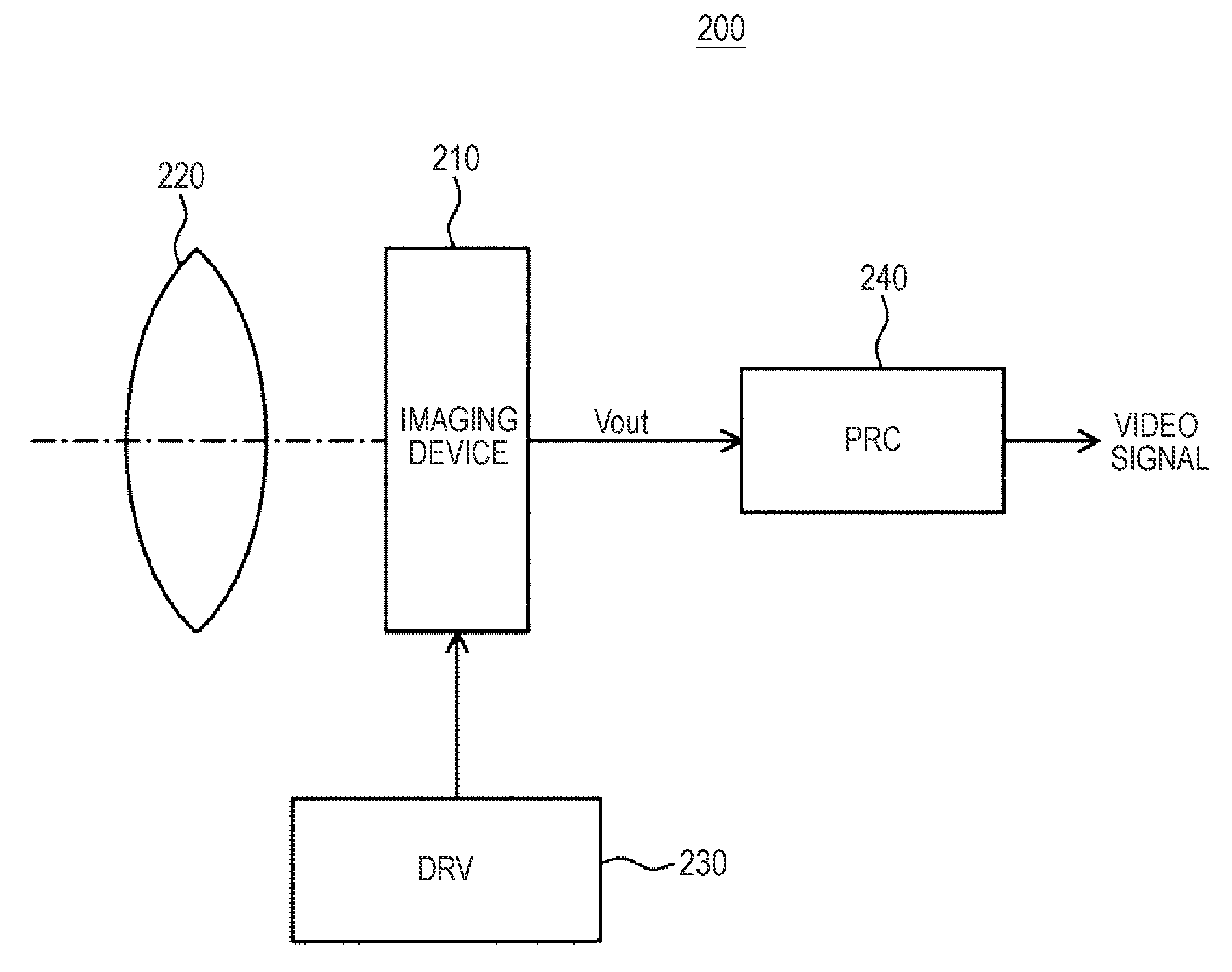
[0055]FIG. 3 is a circuit diagram showing an exemplary configuration of a DA converter according to the first embodiment of the present invention.

[0056]This DA converter 10 according to the first embodiment has an analog output section 11, a current control section 12, a sample and hold circuit section 13, a first bias line LVB11, and a second bias line LVB12.

[0057]The analog output section 11 has a function of generating an output current corresponding to the value of a digital signal in response to a bias voltage and outputting an analog signal which is obtained from the output current by current-to-voltage conversion.

[0058]The analog output section 11 has basic current source cells 11-1 to 11-n, a non-output line L11, an output line L12, and an output resistor R11.

[0059]The DA converter 10 has a sample and hold circuit section 13 that samples and holds a bias voltage Vbias of the basic current source cells 11-1 to ...

second embodiment

2. Second Embodiment

[Second Exemplary Configuration of DA Converter]

[0098]FIG. 5 is a circuit diagram showing an exemplary configuration of a DA converter according to the second embodiment of the present invention.

[0099]This DA converter 10A according to the second embodiment has an analog output section 11A, a current control section 12A, a sample and hold circuit section 13A, a first bias line LVB11A, and a second bias line LVB12A.

[0100]The analog output section 11A has a function of generating an output current corresponding to the value of a digital signal in response to a bias voltage and outputting an analog signal which is obtained from the output current by current-to-voltage conversion.

[0101]The analog output section 11A has basic current source cells 11A-1 to 11A-n, a non-output line L11A, an output line L12A, and an output resistor R11A.

[0102]The DA converter 10A has a sample and hold circuit section 13A that samples and holds a bias voltage Vbias of the basic current so...

third embodiment

3. Third Embodiment

[Third Exemplary Configuration of DA Converter]

[0151]FIG. 8 is a circuit diagram showing an exemplary configuration of a DA converter according to the third embodiment of the present invention.

[0152]This DA converter 10B according to the third embodiment is different from the DA converter 10 according to the first embodiment in the following respects.

[0153]In the DA converter 10B according to the third embodiment, a current control section 12B stops supply of the current of a current source I11B that generates a bias voltage Vbias-s during the hold period of a sample and hold circuit section 13B, thus achieving low power consumption.

[0154]Specifically, in the current control section 12B, a PMOS transistor PT17 is connected in parallel to the PMOS transistor PT14 between the power supply Vdd and a node ND12B which is a connection point of the PMOS transistor PT14 and a current source I11B.

[0155]That is to say, the PMOS transistor PT17 has a drain connected to the n...


PUM


Abstract

A digital-to-analog (DA) converter includes: an analog output section that generates an output current corresponding to a value of a digital signal in response to a bias voltage and outputs an analog signal which is obtained from the output current by current-to-voltage conversion; a current source; a current control section that converts a current from the current source to a voltage signal and outputs the voltage signal as the bias voltage; and a sample and hold circuit section that samples and holds the bias voltage from the current control section and supplies the held bias voltage to the analog output section.

Description

BACKGROUND OF THE INVENTION[0001]1. Field of the Invention[0002]The present invention relates to a DA converter that can be applied to a solid-state imaging device represented by a CMOS image sensor, a solid-state imaging device, and a camera system.[0003]2. Description of the Related Art[0004]A current-controlled digital-to-analog (DA) converter (hereinafter referred to as a DA converter) is generally configured to include a plurality of basic current source cells generating a constant current and an output resistor serving as a current-to-voltage converter.[0005]FIGS. 1A and 1B are diagrams showing an exemplary configuration of a current-controlled DA converter having a basic current source cell.[0006]FIG. 1A shows an exemplary basic configuration of the DA converter when a ground potential GND is used as a reference potential, and FIG. 1B shows an exemplary basic configuration of the DA converter when a power supply potential Vdd is used as a reference potential.[0007]The basic c...

Claims


Application Information

Patent Timeline
Patent Type & Authority Applications(United States)
IPC IPC(8): H04N5/335H03M1/66G06F3/05H04N5/357H04N5/374H04N5/378
CPCH03M1/0607H03M1/0845H03M1/1215H04N5/37455H03M1/56H03M1/742H04N5/3577H03M1/123H04N25/617H04N25/772
Inventor KAWAGUCHI, TAKASHIYOSHIMURA, RYUGI
Owner SONY CORP
Why Eureka
Try Eureka