
Transient Voltage Suppressor Having Symmetrical Breakdown Voltages

a technology of breakdown voltage and transient voltage, which is applied in the direction of electrical equipment, semiconductor devices, circuit arrangements, etc., can solve the problems of large device-to-device variation in breakdown voltage, circuit failure in electronic systems, and breakdown voltage of tv devices that is often not symmetrical

Active Publication Date: 2010-11-04
ALPHA & OMEGA SEMICON INC
View PDF8 Cites 32 Cited by
  • Summary
  • Abstract
  • Description
  • Claims
  • Application Information

AI Technical Summary

Benefits of technology

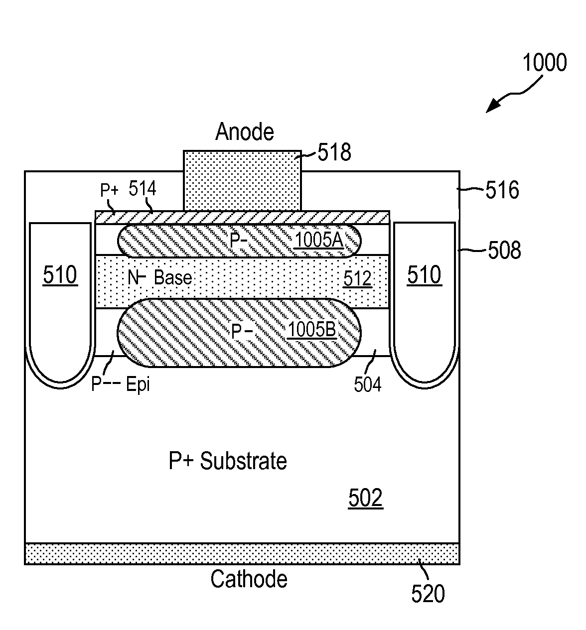
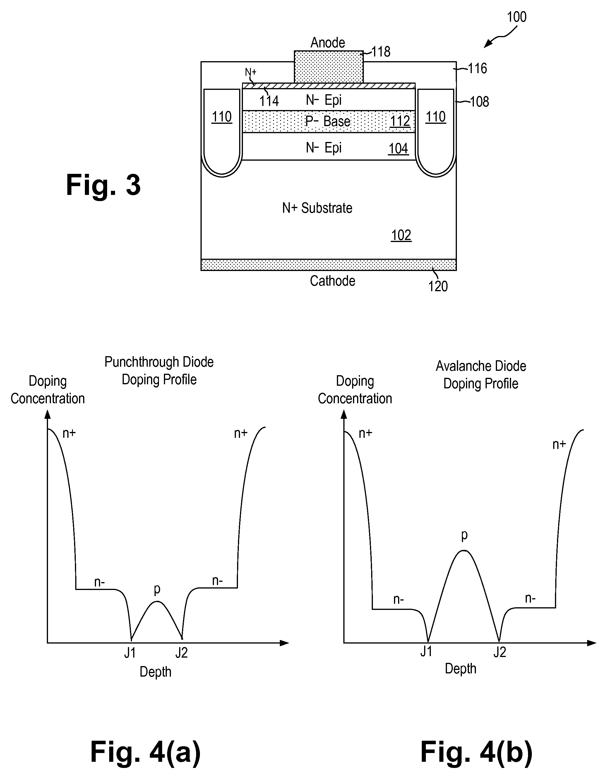
[0008]According to one embodiment of the present invention, a vertical transient voltage suppressing (TVS) device includes a semiconductor substrate of a first conductivity type where the substrate is heavily doped, an epitaxial layer of the first conductivity type formed on the substrate where the epitaxial layer has a first thickness, and a base region of a second conductivity type implanted in the epitaxial layer where the base region is positioned in a middle region of the epitaxial layer. The base region and the epitaxial layer provide a substantially symmetrical vertical doping profile on both sides of the base region such that the breakdown voltages in both directions are symmetrical.

Problems solved by technology

Voltages and current transients are major causes of integrated circuit failure in electronic systems.
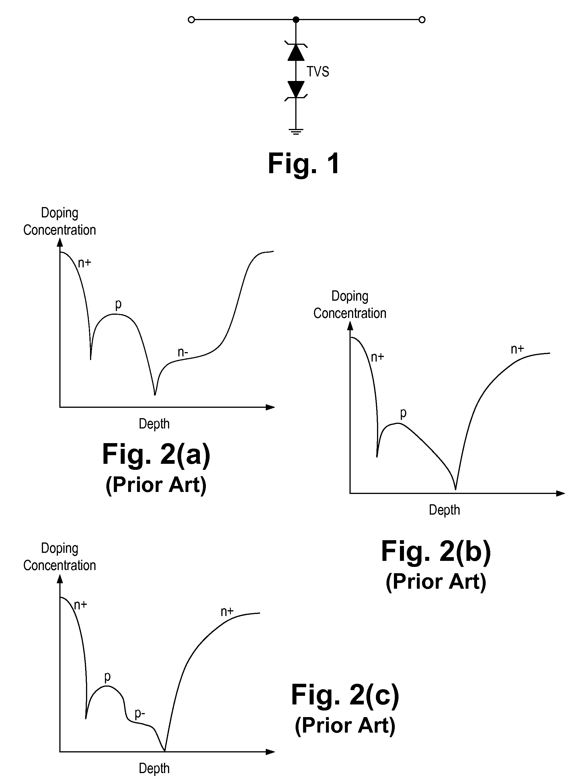
First, due to fabrication process limitation, the breakdown voltage of TVS device is often not symmetrical.
Second, there is often a large device-to-device variation in the breakdown voltages.
Moreover, if the epitaxial layer is too thin, out-doping from the heavily doped substrate can adversely affect the doping concentration of the epitaxial layer or even the base region.
The uneven doping profiles lead to asymmetrical breakdown voltages and breakdown voltages that are sensitive to fabrication process variations.

Method used


Image

  • Transient Voltage Suppressor Having Symmetrical Breakdown Voltages
  • Transient Voltage Suppressor Having Symmetrical Breakdown Voltages
  • Transient Voltage Suppressor Having Symmetrical Breakdown Voltages

Examples


Embodiment Construction

[0029]In accordance with the principles of the present invention, a punchthrough diode based or avalanche mode transient voltage suppressing (TVS) device uses a high energy base implant to form a base region in a thick epitaxial layer to realize a symmetrical NPN or PNP structure. The high energy implantation ensures that the TVS device has a symmetric base doping profile, resulting in a TVS device with symmetrical breakdown voltage. A thick epitaxial layer is used so that when the base region is completely depleted under reverse bias, the depletion layer will not reach the edge of the epitaxial layer, but will remain within the epitaxial layer instead. In this manner, variations in the thickness of the epitaxial layer will not affect the breakdown voltage of the TVS device. In an alternate embodiment, the base region is formed in the middle of the epitaxial layer using a buried layer technology to achieve the same symmetrical doping profile.

[0030]According to another aspect of the ...


PUM


Abstract

A vertical transient voltage suppressing (TVS) device includes a semiconductor substrate of a first conductivity type where the substrate is heavily doped, an epitaxial layer of the first conductivity type formed on the substrate where the epitaxial layer has a first thickness, and a base region of a second conductivity type formed in the epitaxial layer where the base region is positioned in a middle region of the epitaxial layer. The base region and the epitaxial layer provide a substantially symmetrical vertical doping profile on both sides of the base region. In one embodiment, the base region is formed by high energy implantation. In another embodiment, the base region is formed as a buried layer. The doping concentrations of the epitaxial layer and the base region are selected to configure the TVS device as a punchthrough diode based TVS or an avalanche mode TVS.

Description

FIELD OF THE INVENTION[0001]The invention relates to a structure and a method of fabrication of a transient voltage suppressor (TVS) and, in particular, to a structure and a method of fabrication of a vertical transient voltage suppressor (TVS) having symmetrical breakdown voltages and reduced process sensitivity.DESCRIPTION OF THE RELATED ART[0002]Voltages and current transients are major causes of integrated circuit failure in electronic systems. Transients are generated from a variety of sources both internal and external to the system. For instance, common sources of transients include normal switching operations of power supplies, AC line fluctuations, lightning surges, and electrostatic discharge (ESD).[0003]Transient voltage suppressors (TVS) are commonly employed for protecting integrated circuits from damages due to the occurrences of transients or over-voltage conditions at the integrated circuit. TVS devices are either uni-directional devices or bi-directional devices. An...

Claims


Application Information

Patent Timeline
Patent Type & Authority Applications(United States)
IPC IPC(8): H01L29/06H01L21/34H01L21/265H01L21/76H01L21/20
CPCH01L27/0259H01L29/861H01L29/6609H01L29/10
Inventor GUAN, LINGPENGBOBDE, MADHURBHALLA, ANUP
Owner ALPHA & OMEGA SEMICON INC
Learn More